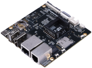
Mainline Linux support for the ARM Primecell PL35X NAND controller

It has been more than 7 years since the first draft of a Linux kernel driver for the ARM Primecell PL35X NAND controller was posted on a public mailing list. Maybe because of the lack of time, each new version was delayed so much that it actually needed another iteration just to catch up with the latest internal API changes in the MTD subsystem (quite a number of them happened in the last 2-3 years). The NAND controller itself is part of an ARM Primecell Static Memory bus Controller (SMC) which increased the overall complexity. Finally, the way the commands and data are shared with the memory controller is very specific to the SMC. All these technical points probably played against Xilinx engineers, and Bootlin was contracted in 2021 to finalize the work of getting the ARM Primecell PL35X NAND controller driver in the upstream Linux kernel.

Static Memory Controller principles

SMC diagram from the TRM

The SMC can interface with two different memory types: NAND or SRAM/NOR. As it features two memory slots, this means that it can drive two memories, but they must be of the same type. When handling NAND devices, a hardware ECC engine is available to perform on-the-fly correction.

As only a single type of memory device can be plugged in at a time (either two SRAM/NORs or two NANDs), we don’t need to share a lot of controls with the SRAM/NOR controllers. So in the end the memory bus driver is almost an empty envelope that relies on the child controller driver to do the job.

Interactions with a memory device

On the CPU side, the controller has two main interfaces: APB and AXI.

The APB interface works like any regular interface: the CPU sees registers that it can access with diverse read and write operations, which will effectively read and write the content of the 32-bit registers located at the desired addresses. This is how the driver configures the device type, the timings, the possible ECC configuration and so forth. All the initial SMC configuration is done through the APB interface.

The AXI interface does not quite work like this. Instead of featuring a set of registers at a fixed address in which the content of the command, address and data cycles would be written in order to be forwarded to the memory device, the AXI interface needs to reserve a notable range in the addressable space. In particular, the offset targetted by the AXI write depend on the type of action that must be performed and the content of the action:

  • When requesting the controller to send command and address cycles to the memory device, the datasheet refers to it as the “command phase”.
  • When doing I/Os, eg. actually reading from/writing to the memory device, the datasheet calls this the “data phase”.

Both the command and data phase use regular AXI read/writes, but the offsets and values are different than usual.

Command phase

When the driver wants to send command cycles, it must perform one or two register writes. The address of the write operation in the AXI address space must target a specific offset. This offset indicates a number of information:

  • A specific bit is set to tell the SMC that it must enter a command phase.
  • Part of the offset are made of the shifted values of the different command opcodes for the memory device.
  • Part of the offset encodes the number of address cycles to perform on the NAND bus.

The payload of the AXI write contains the value of the address cycles that should be forwarded to the memory device. If there are more than 4 address cycles (which is quite common today), then a second AXI write containing the remaining address cycles as payload must happen at the same offset as before.

/*
 * Define the offset in the AXI address space where to write with:
 * - the bit indicating the command phase
 * - the number of address cycles
 * - the command opcode
 */
cmd_addr = PL35X_SMC_CMD_PHASE |
           PL35X_SMC_CMD_PHASE_NADDRS(naddr_cycles) |
           PL35X_SMC_CMD_PHASE_CMD0(NAND_CMD_XXXX);

/* Define the payload with the address bytes */
for (i = 0, row = 0; row < nrows; i++, row++) {
        [...]
        if (row < 4)
                addr1 |= PL35X_SMC_CMD_PHASE_ADDR(row, addr);
        else
                addr2 |= PL35X_SMC_CMD_PHASE_ADDR(row - 4, addr);
}

/* Send the command and address cycles */
writel(addr1, nfc->io_regs + cmd_addr);
if (naddr_cycles > 4)
        writel(addr2, nfc->io_regs + cmd_addr);

Data phase

The data phase is a bit easier to understand: several AXI reads or writes will be performed at a specific offset. The payload matches our expectations: it is actually the data that we want to read from or write to the device. However, the offset in the AXI address space is again a bit counter-intuitive:

  • It contains a specific bit such as the command phase to inform the controller that the data phase must be entered.
  • It also contains shifted values of different flags regarding the ECC configuration. The thing is, this offset will change at the end of the I/O operation because the last chunk of data must always be handled differently because of the ECC calculations that must be manually started. We end up reading or writing physically contiguous data by accessing two completely different offsets.
/* I/O transfers: simple case */
for (i = 0; i < buf_end; i++) {
        data_phase_addr = PL35X_SMC_DATA_PHASE;
        if (i + 1 == buf_end)
                data_phase_addr += PL35X_SMC_DATA_PHASE_ECC_LAST;

        writel(buf32[i], nfc->io_regs + data_phase_addr);
}

But what happens if a command cycle must be sent at the end of a data transfer (typical case of a PAGE_WRITE)? While it would certainly be more logical to perform an additional command phase AXI write, it was certainly more optimized to merge data and command phase on the last access. And here is how it looks like:

/* I/O transfers: less straightforward situation */
for (i = 0; i < buf_end; i++) {
        data_phase_addr = PL35X_SMC_DATA_PHASE;
        if (i + 1 == buf_end)
                data_phase_addr +=
                    PL35X_SMC_DATA_PHASE_ECC_LAST |
                    PL35X_SMC_CMD_PHASE_CMD1(NAND_CMD_PAGEPROG) |
                    PL35X_SMC_CMD_PHASE_CMD1_VALID);

        writel(buf32[i], nfc->io_regs + data_phase_addr);
}

Of course, nothing highly unreadable, but at the very least, these accesses are quite uncommon.

A memory bus driver and a NAND controller driver

As explained earlier, this SMC controller can support different types of memories, and this has called for a Device Tree representation where the SMC controller is one node, and the memories connected to it are represented as sub-node. So, the Device Tree representation of the SMC controller, used with its NAND controller looks like this:

    smcc: memory-controller@e000e000 {
      compatible = "arm,pl353-smc-r2p1", "arm,primecell";
      reg = <0xe000e000 0x0001000>;
      clock-names = "memclk", "apb_pclk";
      clocks = <&clkc 11>, <&clkc 44>;
      ranges = <0x0 0x0 0xe1000000 0x1000000 /* Nand CS region */
                0x1 0x0 0xe2000000 0x2000000 /* SRAM/NOR CS0 region */
                0x2 0x0 0xe4000000 0x2000000>; /* SRAM/NOR CS1 region */
      #address-cells = <2>;
      #size-cells = <1>;

      nfc0: nand-controller@0,0 {
        compatible = "arm,pl353-nand-r2p1";
        reg = <0 0 0x1000000>;
        #address-cells = <1>;
        #size-cells = <0>;
      };
    };

So, we first have a node for the SMC controller itself, memory-controller@e000e000, which will allow probing the memory bus driver located at drivers/memory/pl353-smc.c. This driver is very simple: it enables the clocks necessary for the SMC to work, and then it probes the first child device that matches either the cfi-flash or arm,pl353-nand-r2p1 compatible strings. In the latter case (which is illustrated in our example), the NAND controller driver at drivers/mtd/nand/raw/pl35x-nand-controller.c will be probed, and where the two memory areas (accessed through APB and AXI) will be mapped, and accessed to program the NAND controller.

Now in the mainline Linux kernel

Starting from the latest version posted by Xilinx, Miquèl Raynal, Bootlin’s NAND/MTD expert, performed a massive cleanup of the memory bus driver and the NAND controller driver, rewrote entirely the binding file (in YAML schema!) and three versions later, with the support of Xilinx engineers and the acknowledgements of Rob Herring and Krzysztof Kozlowski, managed to finally close the story. The driver is now part of Linux 5.14-rc, and will therefore be in the final Linux 5.14 release in a few weeks!

GPIO Aggregator, a virtual gpio chip

GPIOs are obviously widely used in embedded systems, and many of them are typically driven directly by Linux kernel drivers for interrupt lines, reset lines, or other control lines used to connect with various peripherals. However, a number of GPIOs are sometimes directly driven by user-space applications. Historically, the Linux kernel has provided a sysfs interface, in /sys/class/gpio to allow such direct control. But in recent years, this sysfs interface has been superseded by a new user-space interface based on /dev/gpiochip* character devices.

This new interface has numerous advantages over the previous /sys/class/gpio interface. However, one drawback is that it creates one device file per GPIO chip, which means that access rights are defined per GPIO chip, and not per GPIOs.

For this reason, in Linux 5.8, Geert Uytterhoeven has contributed the GPIO aggregator mechanism. It allows to group a number of GPIOs into a virtual GPIO chip, visible as an additional /dev/gpiochip*. Its documentation can be found in Documentation/admin-guide/gpio/gpio-aggregator.rst.

The list of GPIOs part of this new virtual GPIO chip is defined in the Device Tree. One other interesting thing is that, as any GPIO controler, the lines can be named, and then queried by user-space applications based on their name, using the libgpiod library.

Configuration and Device Tree description

To have GPIO Aggregator support in your kernel, simply configure

CONFIG_GPIO_AGGREGATOR=y

Add a gpio-aggregator node in your Device Tree source. For instance, the following DTS snippet declares an aggregator with several GPIO lines:

gpio-aggregator {
    pinctrl-names = "default";
    pinctrl-0 = <&gpio_pins>;
    compatible = "gpio-aggregator";

    gpios = <&gpio3 4 GPIO_ACTIVE_HIGH>,
            <&gpio2 4 GPIO_ACTIVE_HIGH>,
            <&gpio1 28 GPIO_ACTIVE_HIGH>,
            <&gpio1 29 GPIO_ACTIVE_HIGH>,
            <&gpio2 0 GPIO_ACTIVE_HIGH>,
            <&gpio2 1 GPIO_ACTIVE_HIGH>,
            <&gpio3 8 GPIO_ACTIVE_HIGH>;

    gpio-line-names = "line_a", "line_b", "line_c", "line_d",
            "line_e", "line_f", "line_g";
};

In this example, line 4 of gpio controller gpio3 is used and is named “line_a”, line 4 of gpio controller gpio2 is used and is named “line_b”, and so on up to line 8 of gpio controler gpio3.

Usage from user-space

From userspace we can see the GPIO chip and its aggregated lines:

# gpioinfo
...
gpiochip6 - 7 lines:
    line 0: "line_a" unused input active-high
    line 1: "line_b" unused input active-high
    line 2: "line_c" unused input active-high
    line 3: "line_d" unused input active-high
    line 4: "line_e" unused input active-high
    line 5: "line_f" unused input active-high
    line 6: "line_g" unused input active-high
...

We can search a gpio chip and a line number by the line name:

# gpiofind 'line_b'
gpiochip6 1

We can access a GPIO line by its name

# gpioget $(gpiofind 'line_b')
1
#
# gpioset $(gpiofind 'line_e')=1
# gpioset $(gpiofind 'line_e')=0

We can change the GPIO chip device file ownership to allow user or group to access the attached lines:

# ls -al /dev/gpiochip*
crw------- 1 root root 254, 0 Jan 1 00:00 /dev/gpiochip0
crw------- 1 root root 254, 1 Jan 1 00:00 /dev/gpiochip1
crw------- 1 root root 254, 2 Jan 1 00:00 /dev/gpiochip2
crw------- 1 root root 254, 3 Jan 1 00:00 /dev/gpiochip3
crw------- 1 root root 254, 4 Jan 1 00:00 /dev/gpiochip4
crw------- 1 root root 254, 5 Jan 1 00:00 /dev/gpiochip5
crw------- 1 root root 254, 6 Jan 1 00:00 /dev/gpiochip6
#
# chown root:users /dev/gpiochip6
# chmod 660 /dev/gpiochip6
# ls -al /dev/gpiochip*
crw------- 1 root root 254, 0 Jan 1 00:00 /dev/gpiochip0
crw------- 1 root root 254, 1 Jan 1 00:00 /dev/gpiochip1
crw------- 1 root root 254, 2 Jan 1 00:00 /dev/gpiochip2
crw------- 1 root root 254, 3 Jan 1 00:00 /dev/gpiochip3
crw------- 1 root root 254, 4 Jan 1 00:00 /dev/gpiochip4
crw------- 1 root root 254, 5 Jan 1 00:00 /dev/gpiochip5
crw-rw---- 1 root users 254, 6 Jan 1 00:00 /dev/gpiochip6
#

The GPIO chip created by the aggregator can be retrieved from sysfs:

# ls -1 /sys/bus/platform/devices/gpio-aggregator/
driver
driver_override
gpio
gpiochip6
modalias
of_node
power
subsystem
uevent
# 
# cat /sys/bus/platform/devices/gpio-aggregator/gpiochip6/dev
254:6
#

Conclusion

A GPIO Aggregator can be used to group a subset of GPIO lines, name them, access them by their names and manage access control to the virtual gpio chip created by the aggregator. On an embedded system, this can simplify the management and usage of individual GPIO lines.

Bootlin contributions to Linux 5.12

Yes, Linux 5.13 was released yesterday, but we never published the blog post detailing our contributions to Linux 5.12, so let’s do this now! First of all the usual links to the excellent LWN.net articles on the 5.12 merge window: part 1 and part 2.

LWN.net also published an article with Linux 5.12 development statistics, and two Bootlin engineers made their way to the statistics: Alexandre Belloni in the list of top contributors by number of changesets, with 69 commits, and Paul Kocialkowski in the list of top contributors by number of changed lines, with over 6000 lines changed.

Here are the highlights of our contributions:

  • Addition of a new driver for the Silvaco I3C master controller. This was contributed by Miquèl Raynal, who became the maintainer for this driver. Bootlin has pioneered support for I3C in Linux, by introducing the complete drivers/i3c subsystem a few years ago, together with the first controller driver, for a Cadence IP, see our blog post from 2018.
  • Addition of two new camera sensor drivers, one for the Omnivision OV5648 and another for the Omnivision OV8865. These were contributed by Paul Kocialkowski.
  • Implementation of mqprio support in the Marvell Ethernet controller driver mvneta, see this commit. As explained in the tc-mqprio man page, the MQPRIO qdisc is a simple queuing discipline that allows mapping traffic flows to hardware queue ranges using priorities and a configurable priority to traffic class mapping. This was contributed by Maxime Chevallier
  • Improvements in the IIO driver for the ms58xx family of sensors, contributed by Alexandre Belloni.
  • The final removal of the atmel_tclib code, which has been replaced by proper drivers for the TCB timers on Atmel/Microchip ARM platforms over the past few releases, also by Alexandre Belloni.
  • As usual, a large amount of fixes and improvements in the RTC subsystem, by its maintainer Alexandre Belloni.

Here is the detailed list of our contributions to this release:

LTP: Linux Test Project, Bootlin contributions

Introduction

The Linux Test Project is a project that develops and maintains a large test suite that helps validating the reliability, robustness and stability of the Linux kernel and related features. LTP has been mainly developed by companies such as IBM, Cisco, Fujitsu, SUSE, RedHat, with a focus on desktop distributions.

On the embedded side, both the openembedded-core Yocto layer and Buildroot have packages that allow to use LTP on embedded targets. However, for a recent project, we practically tried to run the full LTP test suite on an i.MX8 based platform running a Linux system built with Yocto. It turned out that LTP was apparently not very often tested on Busybox-based embedded systems, and we faced a number of issues. In addition to reporting various bugs/issues to the upstream LTP project, we also contributed a number of fixes and improvements:

Our contributions received a very warm welcome in the LTP community, which turned out to be very open and responsive. We hope that these contributions will encourage others to use LTP, and hopefully to make sure it continues to work on embedded platforms.

Quick start guide

At the time of this writing, LTP has more than 3800 tests written by the community, including about 1000 network-related tests. The tests are grouped together in categories described by files in the runtest/ folder. Based on this, two scenarios of tests are defined: default and network which are described by two files in the scenario_groups/ folder. These two scenarios simply list the categories of tests that need to be executed.

Here are the contents of the default and network:

$ cat scenario_groups/default 
syscalls
fs
fs_perms_simple
fsx
dio
io
mm
ipc
sched
math
nptl
pty
containers
fs_bind
controllers
filecaps
cap_bounds
fcntl-locktests
connectors
power_management_tests
hugetlb
commands
hyperthreading
can
cpuhotplug
net.ipv6_lib
input
cve
crypto
kernel_misc
uevent
$ cat scenario_groups/network 
can
net.features
net.ipv6
net.ipv6_lib
net.tcp_cmds
net.multicast
net.rpc
net.nfs
net.rpc_tests
net.tirpc_tests
net.sctp
net_stress.appl
net_stress.broken_ip
net_stress.interface
net_stress.ipsec_dccp
net_stress.ipsec_icmp
net_stress.ipsec_sctp
net_stress.ipsec_tcp
net_stress.ipsec_udp
net_stress.multicast
net_stress.route

Once you have LTP built and installed on your board thanks to the appropriate OpenEmbedded or Buildroot package, you can run these two scenarios of test with the following commands (-n specify the network one):

$ cd /opt/ltp
$ ./runltp
$ ./runltp -n

Then take a look at the content of the result and the output directories.

For more information on building or running LTP please read this readme.

Bootlin contributions to Linux 5.11

Linux 5.11 was released quite some time ago now, but it’s never too late to have a look at Bootlin contributions to this release. As usual, we recommend reading the LWN articles on the 5.11 merge window: part 1 and part2. Also of interest is the Kernelnewbies page for 5.11.

Here are the main highlights of our contributions:

  • Alexandre Belloni, as the maintainer of the RTC subsystem, continued making numerous improvements and fixes to RTC drivers
  • On the support for Microchip ARM platforms, Alexandre Belloni switched the PWM atmel-tcb driver to a new Device Tree binding and added SAMA5D2 support, he did some improvements to the IIO driver for the Microchip ADC, and continued to remove platform_data support from Microchip drivers as all platforms are now converted to the Device Tree.
  • Alexandre Belloni contributed a new Simple Audio Mux driver for the ALSA subsystem, which can be used to control simple audio multiplexers driven using GPIOs, that allows to select which of their input line is connected to the output line.
  • Grégory Clement added support for several new MIPS platforms from Microchip: Luton, Serval and Jaguar2. All those platforms include a MIPS core, a few peripherals and more importantly an Ethernet switch. For now the support only includes the base platform support, but we are working on the switchdev driver for the Ethernet switch.
  • Miquèl Raynal, maintainer of the NAND subsystem and co-maintainer of the MTD subsystem, contributed numerous changes to the ECC support in the MTD subsystem, making it more generic so that it can be used not just for parallel NAND flashes, but also SPI NAND flashes. For more details, see the talk from Miquèl Raynal on this topic.

In addition to those 95 patches that we authored and contributed, several Bootlin engineers being maintainers of different subsystems of the Linux kernel reviewed and merged patches from other contributors:

  • Miquèl Raynal, as the NAND maintainer and MTD co-maintainer, reviewed and merged 67 patches from other contributors
  • Alexandre Belloni, as the RTC, I3C and Microchip ARM/MIPS platforms maintainer, reviewed and merged 47 patches from other contributors
  • Grégory Clement, as the Marvell EBU platform co-maintainer, reviewed and merged 33 patches from other contributors

Here is the detailed list of our contributions to Linux 5.11:

Large Page Support for NAS systems on 32 bit ARM

The need for large page support on 32 bit ARM

Storage space has become more and more affordable to a point that it is now possible to have multiple hard drives of dozens of terabytes in a single consumer-grade device. With a few 10 TiB hard drives and thanks to RAID technology, storage capacities that exceed 16 or 32 TiB can easily be reached and at a relatively low cost.

However, a number of consumer NAS systems used in the field today are still based on 32 bit ARM processors. The problem is that, with Linux on a 32 bit system, it’s only possible to address up to 16 TiB of storage space. This is still true even with the ext4 filesystem, even though it uses 64 bit pointers.

We were lucky to have a customer contracting us to update older Large Page Support patches to a recent version of the Linux kernel. This set of patches are one way of overcoming this 16 TiB limitation for ARM 32-bit systems. Since updating this patch series was a non trivial task, we are happy to share the results of our efforts with the community, both through this blog post and through a patch series we posted to the Linux ARM kernel mailing list: ARM: Add support for large kernel page (from 8K to 64K).

How Large Page Support works

The 16 TiB limitation comes from the use of page->index which is a pgoff_t offset type corresponding to unsigned long. This limits us to a 32-bit page offsets, so with 4 KiB physical pages, we end up with a maximum of 16 TiB. A way to address this limitation is to use larger physical pages. We can reach 32 TiB with 8 KiB pages, 64 TiB with 16 KiB pages and up to 256 TiB with 64 KiB pages.

Before going further, the ARM32 Page Tables article from Linus Walleij is a good reference to understand how the Linux kernel deals with ARM32 page tables. In our case, we are only going to cover the non LPAE case. As explained there, the way the Linux kernel sees the page tables actually doesn’t match reality. First, the kernel deals with 4 levels of page tables while on hardware there are only 2 levels. In addition, while the ARM32 hardware stores only 256 PTEs in Page Tables, taking up only 1 KB, Linux optimizes things by storing in each 4 KB page two sets of 256 PTEs, and two sets of shadow PTEs that are used to store additional metadata needed by Linux about each page (such as the dirty and accessed/young bits). So, there is already some magic between what is presented to the Linux virtual memory management subsystem, and what is really programmed into the hardware page tables. To support large pages, the idea is to go further in this direction by emulating larger physical pages.

Our series (and especially patch 5: ARM: Add large kernel page support) proposes to pretend to have larger hardware pages. The ARM 32-bit architecture only supports 4 KiB or 64 KiB page sizes, but we would like to support intermediate values of 8 KiB, 16 KiB and 32 KiB as well. So what we do to support 8 KiB pages is that we tell Linux the hardware has 8 KiB pages, but in fact we simply use two consecutive 4 KiB pages at the hardware level that we manipulate and configure simultaneously. To support 16 KiB pages, we use 4 consecutive 4 KiB pages, for 32 KiB pages, we use 8 consecutive pages, etc. So really, we “emulate” having larger page sizes by grouping 2, 4 or 8 pages together. Adding this feature only required a few changes in the code, mainly dealing with ranges of pages every time we were dealing with a single page. Actually, most of the code in the series is about making it possible to modify the hard coded value of the hardware page size and fixing the assumptions associated to such a fixed value.

In addition to this emulated mechanism that we provide for 8 KiB, 16 KiB, 32 KiB and 64 KiB pages, we also added support for using real hardware 64 KiB pages as part of this patch series.

Overall the number of changes is very limited (271 lines added, 13 lines removed), and allows to use much larger storage devices. Here is the diffstat of the full patch series:

 arch/arm/include/asm/elf.h                  |  2 +-
 arch/arm/include/asm/fixmap.h               |  3 +-
 arch/arm/include/asm/page.h                 | 12 ++++
 arch/arm/include/asm/pgtable-2level-hwdef.h |  8 +++
 arch/arm/include/asm/pgtable-2level.h       |  6 +-
 arch/arm/include/asm/pgtable.h              |  4 ++
 arch/arm/include/asm/shmparam.h             |  4 ++
 arch/arm/include/asm/tlbflush.h             | 21 +++++-
 arch/arm/kernel/entry-common.S              | 13 ++++
 arch/arm/kernel/traps.c                     | 10 +++
 arch/arm/mm/Kconfig                         | 72 +++++++++++++++++++++
 arch/arm/mm/fault.c                         | 19 ++++++
 arch/arm/mm/mmu.c                           | 22 ++++++-
 arch/arm/mm/pgd.c                           |  2 +
 arch/arm/mm/proc-v7-2level.S                | 72 ++++++++++++++++++++-
 arch/arm/mm/tlb-v7.S                        | 14 +++-
 16 files changed, 271 insertions(+), 13 deletions(-)

This patch series is running in production now on some NAS devices from a very popular NAS brand.

Limitations and alternatives

The submission of our patch series is recent but this feature has actually been running for years on many NAS systems in the field. Our new series is based on the original patchset, with the purpose of submitting it to the mainline kernel community. However, there is little chance that it will ever be merged into the mainline kernel.

The main drawback of this approach are large pages themselves: as each file in the page cache uses at least one page, the memory wasted increases as the size of the pages increases. For this reason, Linus Torvalds was against similar series proposed in the past.

To show how much memory is wasted, Arnd Bergmann ran some numbers to measure the page cache overhead for a typical set of files (Linux 5.7 kernel sources) for 5 different page sizes:

Page size (KiB) 4 8 16 32 64
page cache usage (MiB) 1,023.26 1,209.54 1,628.39 2,557.31 4,550.88
factor over 4K pages 1.00x 1.18x 1.59x 2.50x 4.45x

We can see that while a factor of 1.18 is acceptable for 8 KiB pages, a 4.45 multiplier looks excessive with 64 KiB pages.

Actually, to make it possible to address large volumes on 32 bit ARM, another solution was pointed out during the review of our series. Instead of using larger pages which have an impact on the entire system, an alternative is to modify the way the filesystem addresses the memory by using 64 bits pgoff_t offsets. This has already been implemented in vendor kernels running in some NAS systems, but this has never been submitted to mainline developers.

Videos and slides from Bootlin talks at Embedded Linux Conference Europe 2020

The Embedded Linux Conference Europe took place online last week. While we definitely missed the experience of an in-person event, we strongly participated to this conference with no less than 7 talks on various topics showing Bootlin expertise in different fields: Linux kernel development in networking, multimedia and storage, but also build systems and tooling. We’re happy to be publishing now the slides and videos of our talks.

From the camera sensor to the user: the journey of a video frame, Maxime Chevallier

Download the slides: PDF, source.

OpenEmbedded and Yocto Project best practices, Alexandre Belloni

Download the slides: PDF, source.

Supporting hardware-accelerated video encoding with mainline Linux, Paul Kocialkowski

Download the slides: PDF, source.

Building embedded Debian/Ubuntu systems with ELBE, Köry Maincent

Download the slides: PDF, source.

Understand ECC support for NAND flash devices in Linux, Miquèl Raynal

Download the slides: PDF, source.

Using Visual Studio Code for Embedded Linux Development, Michael Opdenacker

Download the slides: PDF, source.

Precision Time Protocol (PTP) and packet timestamping in Linux, Antoine Ténart

Download the slides: PDF, source.

Supporting a misbehaving NAND ECC engine

Over the years, Bootlin has grown a significant expertise in U-Boot and Linux support for flash memory devices. Thanks to this expertise, we have recently been in charge of rewriting and upstreaming a driver for the Arasan NAND controller, which is used in a number of Xilinx Zynq SoCs. It turned out that supporting this NAND controller had some interesting challenges to handle its ECC engine peculiarities. In this blog post, we would like to give some background about ECC issues with NAND flash devices, and then dive into the specific issues that we encountered with the Arasan NAND controller, and how we solved them.

Ensuring data integrity

NAND flash memories are known to be intrinsically rather unstable: over time, external conditions or repetitive access to a NAND device may result in the data being corrupted. This is particularly true with newer chips, where the number of corruptions usually increases with density, requiring even stronger corrections. To mitigate this, Error Correcting Codes are typically used to detect and correct such corruptions, and since the calculations related to ECC detection and correction are quite intensive, NAND controllers often embed a dedicated engine, the ECC engine, to offload those operations from the CPU.

An ECC engine typically acts as a DMA master, moving, correcting data and calculating syndromes on the fly between the controller FIFO’s and the user buffer. The engine correction is characterized by two inputs: the size of the data chunks on which the correction applies and the strength of the correction. Old SLC (Single Level Cell) NAND chips typically require a strength of 1 symbol over 4096 (1 bit/512 bytes) while new ones may require much more: 8, 16 or even 24 symbols.

In the write path, the ECC engine reads a user buffer and computes a code for each chunk of data. NAND pages being longer than officially advertised, there is a persistent Out-Of-Band (OOB) area which may be used to store these codes. When reading data, the ECC engine gets fed by the data coming from the NAND bus, including the OOB area. Chunk by chunk, the engine will do some math and correct the data if needed, and then report the number of corrected symbols. If the number of error is higher than the chosen strength, the engine is not capable of any correction and returns an error.

The Arasan ECC engine

As explained in our introduction, as part of our work on upstreaming the Arasan NAND controller driver, we discovered that this NAND controller IP has a specific behavior in terms of how it reports ECC results: the hardware ECC engine never reports errors. It means the data may be corrected or uncorrectable: the engine behaves the same. From a software point of view, this is a critical flaw and fully relying on such hardware was not an option.

To overcome this limitation, we investigated different solutions, which we detail in the sections below.

Suppose there will never be any uncorrectable error

Let’s be honest, this hypothesis is highly unreliable. Besides that anyway, it would imply that we do not differentiate between written/erased pages and users would receive unclean buffers (with bitflips), which would not work with upper layers such as UBI/UBIFS which expect clean data.

Keep an history of bitflips of every page

This way, during a read, it would be possible to compare the evolution of the number of bitflips. If it suddenly drops significantly, the engine is lying and we are facing an error. Unfortunately it is not a reliable solution either because we should either trigger a write operation every time a read happens (slowing down a lot the I/Os and wearing out very quickly the storage device) or loose the tracking after every power cycle which would make this solution very fragile.

Add a CRC16

This CRC16 could lay in the OOB area and help to manually verify the data integrity after the engine’s correction by checking it against the checksum. This could be acceptable, even if not perfect in term of collisions. However, it would not work with existing data while there are many downstreams users of the vendor driver already.

Use a bitwise XOR between raw and corrected data

By doing a bitwise XOR between raw and corrected datra, and compare with the number of bitflips reported by the engine, we could detect if the engine is lying on the number of corrected bitflips. This solution has actually been implemented and tested. It involves extra I/Os as the page must be read twice: first with correction and then again without correction. Hence, the NAND bus throughput becomes a limiting factor. In addition, when there are too many bitflips, the engine still tries to correct data and creates bitflips by itself. The result is that, with just a XOR, we cannot discriminate a working correction from a failure. The following figure shows the issue.

Show the engine issue when it creates bitflips when trying to correct uncorrectable data

Rely on the hardware only in the write path

Using the hardware engine in the write path is fine (and possibly the quickest solution). Instead of trying to workaround the flaws of the read path, we can do the math by software to derive the syndrome in the read path and compare it with the one in the OOB section. If it does not match, it means we are facing an uncorrectable error. This is finally the solution that we have chosen. Of course, if we want to compare software and hardware calculated ECC bytes, we must find a way to reproduce the hardware calculations, and this is what we are going to explore in the next sections.

Reversing a hardware BCH ECC engine

There is already a BCH library in the Linux kernel on which we could rely on to compute BCH codes. What needed to be identified though, were the BCH initial parameters. In particular:

  • The BCH primary polynomial, from which is derived the generator polynomial. The latter is then used for the computation of BCH codes.
  • The range of data on which the derivation would apply.

There are several thousands possible primary polynomials with a form like x^3 + x^2 + 1. In order to represent these polynomials more easily by software, we use integers or binary arrays. In both cases, each bit represents the coefficient for the order of magnitude corresponding to its position. The above example could be represented by b1101 or 0xD.

For a given desired BCH code (ie. the ECC chunk size and hence its corresponding Gallois Field order), there is a limited range of possible primary polynomials which can be used. Given eccsize being the amount of data to protect, the Gallois Field order is the smallest integer m so that: 2^m > eccsize. Knowing m, one can check these tables to see examples of polynomials which could match (non exhaustive). The Arasan ECC engine supporting two possible ECC chunk sizes of 512 and 1024 bytes, we had to look at the tables for m = 13 and m = 14.

Given the required strength t, the number of needed parity bits p is: p = t x m.

The total amount of manipulated data (ECC chunk, parity bits, eventual padding) n, also called BCH codeword in papers, is: n = 2^m - 1.

Given the size of the codeword n and the number of parity bits p, it is then possible to derive the maximum message length k with: k = n - p.

The theory of BCH also shows that if (n, k) is a valid BCH code, then (n - x, k - x) will also be valid. In our situation this is very interesting. Indeed, we want to protect eccsize number of symbols, but we currently cover k within n. In other words we could use the translation factor x being: x = k - eccsize. If the ECC engine was also protecting some part of the OOB area, x should have been extended a little bit to match the extra range.

With all this theory in mind, we used GNU Octave to brute force the BCH polynomials used by the Arasan ECC engine with the following logic:

  • Write a NAND page with a eccsize-long ECC step full of zeros, and another one full of ones: this is our known set of inputs.
  • Extract each BCH code of p bits produced by the hardware: this is our known set of outputs.

For each possible primary polynomial with the Gallois Field order m, we derive a generator polynomial, use it to encode both input buffers thanks to a regular BCH derivation, and compare the output syndromes with the expected output buffers.

Because the GNU Octave program was not tricky to write, we first tried to match with the output of Linux software BCH engine. Linux using by default the primary polynomial which is the first in GNU Octave’s list for the desired field order, it was quite easy to verify the algorithm worked.

As unfortunate as it sounds, running this test with the hardware data did not gave any match. Looking more in depth, we realized that visually, there was something like a matching pattern between the output of the Arasan engine and the output of Linux software BCH engine. In fact, both syndromes where identical, the bits being swapped at byte level by the hardware. This observation was made possible because the input buffers have the same values no matter the bit ordering. By extension, we also figured that swapping the bits in the input buffer was also necessary.

The primary polynomial for an eccsize of 512 bytes being already found, we ran again the program with eccsize being 1024 bytes:

eccsize = 1024
eccstrength = 24
m = 14
n = 16383
p = 336
k = 16047
x = 7855
Trying primary polynomial #1: 0x402b
Trying primary polynomial #2: 0x4039
Trying primary polynomial #3: 0x4053
Trying primary polynomial #4: 0x405f
Trying primary polynomial #5: 0x407b
[...]
Trying primary polynomial #44: 0x43c9
Trying primary polynomial #45: 0x43eb
Trying primary polynomial #46: 0x43ed
Trying primary polynomial #47: 0x440b
Trying primary polynomial #48: 0x4443
Primary polynomial found! 0x4443

Final solution

With the two possible primary polynomials in hand, we could finish the support for this ECC engine.

At first, we tried a “mixed-mode” solution: read and correct the data with the hardware engine and then re-read the data in raw mode. Calculate the syndrome over the raw data, derive the number of roots of the syndrome which represents the number of bitflips and compare with the hardware engine’s output. As finding the syndrome’s roots location (ie. the bitflips offsets) is very time consuming for the machine it was decided not to do it in order to gain some time. This approach worked, but doing the I/Os twice was slowing down very much the read speed, much more than expected.

The final approach has been to actually get rid of any hardware computation in the read path, delegating all the work to Linux BCH logic, which indeed worked noticeably faster.

The overall work is now in the upstream Linux kernel:

If you’re interested about more details on ECC for flash devices, and their support in Linux, we will be giving a talk precisely on this topic at the upcoming Embedded Linux Conference!

Practical usage of timer counters in Linux, illustrated on Microchip platforms

Virtually all micro-controllers and micro-processors provide some form of timer counters. In the context of Linux, they are always used for kernel timers, but they can also sometimes be used for PWMs, or input capture devices able to measure external signals such as rotary encoders. In this blog post, we would like to illustrate how Linux can take advantage of such timer counters, by taking the example of the Microchip Timer Counter Block, and depict how its various features fit into existing Linux kernel subsystems.

Hardware overview

On Microchip ARM processors, the TCB (Timer Counter Block) module is a set of three independent, 16 or 32-bits, channels as illustrated in this simplified block diagram:

Microchip TCB

The exact number of TCB modules depends on which Microchip processor you’re using, this Microchip brochure gives the details. Most products have 6 or 9 timer counter channels available, which are grouped into two or three TCB modules, each having 3 channels.

Each TC channel can independently select a clock source for its counter:

  • Internal Clock: sourced from either the system bus clock (often the highest rated one with pre-defined divisors), the slow clock (crystal oscillator) and for the Microchip SAMA5D2 and SAM9X60 SOC series there is even a programmable generic clock source (GCLK) specific to each peripheral.
  • External Clock: based on the three available external input pins: TCLK0, TCLK1 or TCLK2.

The clock source choice should obviously be made depending on the accuracy required by the application.

The module has many functions declined in three different modes:

  • The input capture mode is useful to capture input signals (e.g measure a signal period) through one of the six input pins (TIOAx/TIOBx) connected to each TC module. Each pin can act as trigger source for the counter and two latch register RA/RB can be loaded and compared with a third RC register. This mode is highly configurable with lots of feature to fine tune the capture (subsambling, clock inverting, interrupt, etc.).
  • The waveform mode which provide the core function of TCs as all channels could be used as three independent free-running counters and it is also a mode used to generate PWM signals which gives an extra pool of PWMs
  • The quadrature mode is only supported on the first TC module TCB0 and two (or three) channels are required, channel 0 will decode the speed or position on TIOA0/TIOB0, channel 1 (with TIOB1 input) can be configured to store the revolution or number of rotation. Finally if speed measurement is configured the channel 2 shall define a speed time base.Something important to note is that this mode actually is only part of Microchip SAMA5 and SAM9x60 family SOCs.

Software overview

On the software side in the Linux kernel, the different functionalities offered by the Microchip TCBs will be handled by three different subsystems, which we cover in the following sections.

Clocksource susbsystem

This subsystem is the core target of any TC module as it allows the kernel to keep track of the time passing (clocksource) and program timer interrupts (clockevents). The Microchip TCB has its upstream implementation in drivers/clocksource/timer-atmel-tcb.c that uses the waveform mode to provide both clock source and clock events. The older Microchip platforms have only 16-bit timer counters, in which case two channels are needed to implement the clocksource support. Newer Microchip platforms have 32-bit timer counters, and in this case only one channel is needed to implement clocksource. In both cases, only one channel is necessary to implement clock events.

In the timer-atmel-tcb driver:

  • The clocksource is registered using a struct clocksource structure which mainly provides a ->read() callback to read the current cycle count
  • The clockevents is registered using a struct tc_clkevt_device structure, which provides callbacks to set the date of the next timer event (->set_next_event()) and to change the mode of the timer (->set_state_shutdown(), ->set_state_periodic(), ->set_state_oneshot()).

From a user-space point of view, the clocksource and clockevents subsystems are not directly visible, but they are of course used whenever one uses time or timer related functions. The available clockevents are visible in /sys/bus/clockevents and the available clocksources are visible in /sys/bus/clocksource. The file /proc/timer_list also gives a lot of information about the timers that are pending, and the available timer devices on the platform.

PWM subsystem

This subsystem is useful for many applications (fan control, leds, beepers etc.), and provides both an in-kernel APIs for other kernel drivers to use, as well as a user-space API in /sys/class/pwm, documented at https://www.kernel.org/doc/html/latest/driver-api/pwm.html.

As far as PWM functionality is concerned, the Microchip TCB module is supported by the driver at drivers/pwm/pwm-atmel-tcb.c, which also uses the waveform mode. In this mode both channels pins TIOAx/TIOBx can be used to output PWM signals which allows to provide up to 6 PWM outputs per TCB. On a high-level, this PWM driver registers a struct pwm_ops structure that provides pointers to the important callback to setup and configure PWM outputs.

The current diver implementation has the drawback of using an entire TCB module as a PWM chip: it is not possible to use 1 channel of a TCB module for PWM, and the other channels of the same TCB module for other functionality. On platforms that have only two TCB modules, this means that the first TCB module is typically used for the clockevents/clocksource functionality described previously, and therefore only the second TCB module can be used for PWM.

We are however working on lifting this limitation: Bootlin engineer Alexandre Belloni has a patch series at https://github.com/alexandrebelloni/linux/commits/at91-tcb to address this. We aim at submitting this patch series in the near future.

Thanks to the changes of this patch series, we will be able to use PWM channels as follows:

  • Configuring a 100KHz PWM signal on TIOAx:
    # echo 0 > /sys/class/pwm/pwmchip0/export
    # echo 10000 > /sys/class/pwm/pwmchip0/pwm0/period
    # echo 1000 > /sys/class/pwm/pwmchip0/pwm0/duty_cycle
    # echo 1 > /sys/class/pwm/pwmchip0/pwm0/enable
    
  • Configuring a 100KHz PWM signal on TIOBx:
    # echo 1 > /sys/class/pwm/pwmchip0/export
    # echo 10000 > /sys/class/pwm/pwmchip0/pwm1/period
    # echo 1000 > /sys/class/pwm/pwmchip0/pwm1/duty_cycle
    # echo 1 > /sys/class/pwm/pwmchip0/pwm1/enable
    
  • One must note that both PWM signals of the same channel will share the same period even though we set it twice here as it is required by the PWM framework. The Microchip TCB takes the period from the RC register and RA/RB respectively for TIOAx/TIOBx duty cycles.

    Counter subsystem

    The Linux kernel counter subsystem, located in drivers/counter/ is much newer than the clocksource, clockevents and PWM subsystems described previously. Indeed, it is only in 2019 that it was added to the Linux kernel, and so far it contains only 5 drivers. This subsystem abstracts a timer counter as three entities: a Count that stores the value incremented or decremented from a measured input Signal and a Synapse that will provide edge-based trigger source.

    This subsystem was therefore very relevant to expose the input capture and quadrature decoder modes of the Microchip TCB module, and we recently submitted a patch series that implements a counter driver for the Microchip TCB module. The driver instantiates and registers a struct counter_device structure, with a variety of sub-structures and callbacks that allow the core counter subsystem to use the Microchip TCB module and expose its input capture and quadrature decoder features to user-space.

    The current user-space interface of the counter subsystem works over sysfs and is documented at https://www.kernel.org/doc/html/latest/driver-api/generic-counter.html. For example, to read the position of a rotary encoder connected to a TCB module configured as a quadradure decoder, one would do:

    # cd /sys/bus/counter/devices/counter0/count0/                    
    # echo "quadrature x4" > function                                 
    # cat count
    0
    

    However, when the device connected to the TCB is a rotary encoder, it would be much more useful to have it exposed to user-space as a standard input device so that all existing graphical libraries and frameworks can automatically make use of it. Rotary encoders connected to GPIOs can already be exposed to user-space as input devices using the rotary_encoder driver. Our goal was to achieve the same, but with a rotary encoder connected to a quadrature decoder handled by the counter subsystem. To this end, we submitted a second patch series, which:

    1. Extends the counter subsystem with an in-kernel API, so that counter devices can not only be used from user-space using sysfs, but also from other kernel subsystems. This is very much like the IIO in-kernel API, which is used in a variety of other kernel subsystems that need access to IIO devices.
    2. A new rotary-encoder-counter driver, which implements an input device based on a counter device configured in quadrature decoder mode.

    Thanks to this driver, we get an input device for our rotary encoder, which can for example be tested using evtest to decode the input events that occur when rotating the rotary encoder:

    # evtest /dev/input/event1                                        
    Input driver version is 1.0.1                                     
    Input device ID: bus 0x19 vendor 0x0 product 0x0 version 0x0      
    Input device name: "rotary@0"                                     
    Supported events:                                                 
    Event type 0 (EV_SYN)                                           
    Event type 2 (EV_REL)                                           
      Event code 0 (REL_X)                                          
    Properties:                                                       
    Testing ... (interrupt to exit)                                   
    Event: time 1325392910.906948, type 2 (EV_REL), code 0 (REL_X), value 2
    Event: time 1325392910.906948, -------------- SYN_REPORT ------------
    Event: time 1325392911.416973, type 2 (EV_REL), code 0 (REL_X), value 1
    Event: time 1325392911.416973, -------------- SYN_REPORT ------------
    Event: time 1325392913.456956, type 2 (EV_REL), code 0 (REL_X), value 2
    Event: time 1325392913.456956, -------------- SYN_REPORT ------------
    Event: time 1325392916.006937, type 2 (EV_REL), code 0 (REL_X), value 1
    Event: time 1325392916.006937, -------------- SYN_REPORT ------------
    Event: time 1325392919.066977, type 2 (EV_REL), code 0 (REL_X), value 1
    Event: time 1325392919.066977, -------------- SYN_REPORT ------------
    Event: time 1325392919.576988, type 2 (EV_REL), code 0 (REL_X), value 2
    Event: time 1325392919.576988, -------------- SYN_REPORT ------------      
    

    Device Tree

    From a Device Tree point of view, the representation is a bit more complicated than for many other hardware blocks, due to the multiple features offered by timer counters. First of all, in the .dtsi file describing the system-on-chip, we have a node that describes each TCB module. For example, for the Microchip SAMA5D2 system-on-chip, which has two TCB modules, we have in arch/arm/boot/dts/sama5d2.dtsi:

    tcb0: timer@f800c000 {
    	compatible = "atmel,at91sam9x5-tcb", "simple-mfd", "syscon";
    	#address-cells = <1>;
    	#size-cells = <0>;
    	reg = <0xf800c000 0x100>;
    	interrupts = <35 IRQ_TYPE_LEVEL_HIGH 0>;
    	clocks = <&pmc PMC_TYPE_PERIPHERAL 35>, <&clk32k>;
    	clock-names = "t0_clk", "slow_clk";
    };
    
    tcb1: timer@f8010000 {
    	compatible = "atmel,at91sam9x5-tcb", "simple-mfd", "syscon";
    	#address-cells = <1>;
    	#size-cells = <0>;
    	reg = <0xf8010000 0x100>;
    	interrupts = <36 IRQ_TYPE_LEVEL_HIGH 0>;
    	clocks = <&pmc PMC_TYPE_PERIPHERAL 36>, <&clk32k>;
    	clock-names = "t0_clk", "slow_clk";
    };
    

    This however does not define how each TCB module and each channel is going to be used. This happens at the board level, by adding sub-nodes to the appropriate TCB module node.

    First, each board needs to at least define which TCB module and channels should be used for the clocksource/clockevents. For example, arch/arm/boot/dts/at91-sama5d2_xplained.dts has:

    tcb0: timer@f800c000 {
    	timer0: timer@0 {
    		compatible = "atmel,tcb-timer";
    		reg = <0>;
    	};
    
    	timer1: timer@1 {
    		compatible = "atmel,tcb-timer";
    		reg = <1>;
    	};
    };
    

    As can be seen in this example, the timer@0 and timer@1 node are sub-nodes of the timer@f800c000 node. The SAMA5D2 has 32-bit timer counters, so only one channel is needed for the clocksource, and another channel is needed for clock events. Older platforms such as AT91SAM9260 would need:

    tcb0: timer@fffa0000 {
    	timer@0 {
    		compatible = "atmel,tcb-timer";
    		reg = <0>, <1>;
    	};
    
    	timer@2 {
    		compatible = "atmel,tcb-timer";
    		reg = <2>;
    	};
    };
    

    Where the first instance of atmel,tcb-timer uses two channels: on AT91SAM9260, each channel is only 16-bit, so we need two channels for clocksource. This is why we have reg = <0>, <1> in the first sub-node.

    Now, to use some TCB channels as PWMs, with the new patch series proposed by Alexandre, one would for example use:

    &tcb1 {
    	tcb1_pwm0: pwm@0 {
    		compatible = "atmel,tcb-pwm";
    		#pwm-cells = <3>;
    		reg = <0>;
    		pinctrl-names = "default";
    		pinctrl-0 = <&pinctrl_tcb1_tioa0 &pinctrl_tcb1_tiob0>;
    	};
    
    	tcb1_pwm1: pwm@1 {
    		compatible = "atmel,tcb-pwm";
    		#pwm-cells = <3>;
    		reg = <1>;
    		pinctrl-names = "default";
    		pinctrl-0 = <&pinctrl_tcb1_tioa1>;
    	};
    };
    

    To use the two first channels of TCB1 as PWMs. This would provide two separate PWM devices visible to user-space, and to other kernel drivers.

    Otherwise, to use a TCB as a quadrature decoder, one would use the following piece of Device Tree. Note that we must use the TCB0 module as it is the only one that supports quadrature decoding. This means that the atmel,tcb-timer nodes for clocksource/clockevents support have to use TCB1.

    &tcb0 {
    	qdec: counter@0 {
    		compatible = "atmel,tcb-capture";
    		reg = <0>, <1>;
    		pinctrl-names = "default";
    		pinctrl-0 = <&pinctrl_qdec_default>;
    	};
    };
    

    A quadrature decoder needs two channels, hence the reg = <0>, <1>.

    And if in addition you would like to setup an input device for the rotary encoder connected to the quadrature decoder, you can add:

    rotary@0 {
    	compatible = "rotary-encoder-counter";
    	counter = <&qdec>;
    	qdec-mode = <7>;
    	poll-interval = <50>;
    };
    

    Note that this is not a sub-node of the TCB node, the rotary encoder needs to be described at the top-level of the Device Tree, and has a reference to the TCB channels used as quadrature decoder by means of the counter = <&qdec>; phandle.

    Of course, these different capabilities can be combined. For example, you could use the first two channels of TCB0 to implement a quadrature decoder using the counter subsystem, and the third channel of the same TCB module for a PWM. TCB1 is used for clocksource/clockevents. In this case, the Device Tree would look like this:

    &tcb0 {
    	counter@0 {
    		compatible = "atmel,tcb-capture";
    		reg = <0>, <1>;
    		pinctrl-names = "default";
    		pinctrl-0 = <&pinctrl_qdec_default>;
    	};
    
    	pwm@2 {
    		compatible = "atmel,tcb-pwm";
    		#pwm-cells = <3>;
    		reg = <2>;
    		pinctrl-names = "default";
    		pinctrl-0 = <&pinctrl_tcb1_tioa1>;
    	};
    };
    
    &tcb1 {
    	timer@0 {
    		compatible = "atmel,tcb-timer";
    		reg = <0>, <1>;
    	};
    
    	timer@2 {
    		compatible = "atmel,tcb-timer";
    		reg = <2>;
    	};
    };
    

    Conclusion

    We hope that this blog post was useful to understand how Linux handles timer counters, and what are the Linux kernel subsystems that are involved. Even though we used the Microchip TCB to illustrate our discussion, the concepts all apply to the timer counters of other platforms that would offer similar features.

Linux 5.6, Bootlin contributions inside

Linux 5.6 was released last Sunday. As usual, LWN has the best coverage of the new features merged in this release: part 1 and part 2. Sadly, the corresponding KernelNewbies page has not yet been updated with the usual very interesting summary of the important changes.

Bootlin contributed a total of 95 patches to this release, which makes us the 27th contributing company by number of commits, according to the statistics. The main highlights of our contributions are:

  • Our work on supporting hardware-offloading of MACsec encryption/decryption in the networking subsystem and support for this offloading for some Microchip/Vitesse PHYs has been merged. See our previous blog post for more details about this work done by Bootlin engineer Antoine Ténart
  • As part of our work on the Rockchip PX30 system-on-chip, we contributed support for LVDS display on Rockchip PX30, and support for the Satoz SAT050AT40H12R2 panel. This work was done by Miquèl Raynal
  • Alexandre Belloni as the RTC maintainer did his usual number of cleanup and improvements to existing RTC drivers
  • We did a number of small contributions to the Microchip AT91/SAMA5 platform: support for the Smartkiz platform from Overkiz, phylink improvements in the macb driver, etc.
  • Paul Kocialkowski improved the Intel GMA 500 DRM driver to support page flip.
  • Paul Kocialkowski contributed support for the Xylon LogiCVC GPIO controller, which is a preliminary step to contributing the Xylon LogiCVC display controller support. See our blog post on this topic.

In addition to being contributors, a number of Bootlin engineers are also maintainers of various parts of the Linux kernel, and as such:

  • Alexandre Belloni, as the RTC subsystem maintainer and Microchip platforms co-maintainer, has reviewed and merged 55 patches from other contributors
  • Miquèl Raynal, as the MTD co-maintainer, has reviewed and merged 21 patches from other contributors
  • Grégory Clement, as the Marvell EBU platform co-maintainer, has reviewed and merged 12 patches from other contributors

Here is the detail of all our contributions: