Mainline Linux support for the ARM Primecell PL35X NAND controller

It has been more than 7 years since the first draft of a Linux kernel driver for the ARM Primecell PL35X NAND controller was posted on a public mailing list. Maybe because of the lack of time, each new version was delayed so much that it actually needed another iteration just to catch up with the latest internal API changes in the MTD subsystem (quite a number of them happened in the last 2-3 years). The NAND controller itself is part of an ARM Primecell Static Memory bus Controller (SMC) which increased the overall complexity. Finally, the way the commands and data are shared with the memory controller is very specific to the SMC. All these technical points probably played against Xilinx engineers, and Bootlin was contracted in 2021 to finalize the work of getting the ARM Primecell PL35X NAND controller driver in the upstream Linux kernel.

Static Memory Controller principles

SMC diagram from the TRM

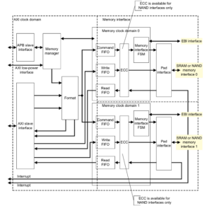
The SMC can interface with two different memory types: NAND or SRAM/NOR. As it features two memory slots, this means that it can drive two memories, but they must be of the same type. When handling NAND devices, a hardware ECC engine is available to perform on-the-fly correction.

As only a single type of memory device can be plugged in at a time (either two SRAM/NORs or two NANDs), we don’t need to share a lot of controls with the SRAM/NOR controllers. So in the end the memory bus driver is almost an empty envelope that relies on the child controller driver to do the job.

Interactions with a memory device

On the CPU side, the controller has two main interfaces: APB and AXI.

The APB interface works like any regular interface: the CPU sees registers that it can access with diverse read and write operations, which will effectively read and write the content of the 32-bit registers located at the desired addresses. This is how the driver configures the device type, the timings, the possible ECC configuration and so forth. All the initial SMC configuration is done through the APB interface.

The AXI interface does not quite work like this. Instead of featuring a set of registers at a fixed address in which the content of the command, address and data cycles would be written in order to be forwarded to the memory device, the AXI interface needs to reserve a notable range in the addressable space. In particular, the offset targetted by the AXI write depend on the type of action that must be performed and the content of the action:

  • When requesting the controller to send command and address cycles to the memory device, the datasheet refers to it as the “command phase”.
  • When doing I/Os, eg. actually reading from/writing to the memory device, the datasheet calls this the “data phase”.

Both the command and data phase use regular AXI read/writes, but the offsets and values are different than usual.

Command phase

When the driver wants to send command cycles, it must perform one or two register writes. The address of the write operation in the AXI address space must target a specific offset. This offset indicates a number of information:

  • A specific bit is set to tell the SMC that it must enter a command phase.
  • Part of the offset are made of the shifted values of the different command opcodes for the memory device.
  • Part of the offset encodes the number of address cycles to perform on the NAND bus.

The payload of the AXI write contains the value of the address cycles that should be forwarded to the memory device. If there are more than 4 address cycles (which is quite common today), then a second AXI write containing the remaining address cycles as payload must happen at the same offset as before.

/*
 * Define the offset in the AXI address space where to write with:
 * - the bit indicating the command phase
 * - the number of address cycles
 * - the command opcode
 */
cmd_addr = PL35X_SMC_CMD_PHASE |
           PL35X_SMC_CMD_PHASE_NADDRS(naddr_cycles) |
           PL35X_SMC_CMD_PHASE_CMD0(NAND_CMD_XXXX);

/* Define the payload with the address bytes */
for (i = 0, row = 0; row < nrows; i++, row++) {
        [...]
        if (row < 4)
                addr1 |= PL35X_SMC_CMD_PHASE_ADDR(row, addr);
        else
                addr2 |= PL35X_SMC_CMD_PHASE_ADDR(row - 4, addr);
}

/* Send the command and address cycles */
writel(addr1, nfc->io_regs + cmd_addr);
if (naddr_cycles > 4)
        writel(addr2, nfc->io_regs + cmd_addr);

Data phase

The data phase is a bit easier to understand: several AXI reads or writes will be performed at a specific offset. The payload matches our expectations: it is actually the data that we want to read from or write to the device. However, the offset in the AXI address space is again a bit counter-intuitive:

  • It contains a specific bit such as the command phase to inform the controller that the data phase must be entered.
  • It also contains shifted values of different flags regarding the ECC configuration. The thing is, this offset will change at the end of the I/O operation because the last chunk of data must always be handled differently because of the ECC calculations that must be manually started. We end up reading or writing physically contiguous data by accessing two completely different offsets.
/* I/O transfers: simple case */
for (i = 0; i < buf_end; i++) {
        data_phase_addr = PL35X_SMC_DATA_PHASE;
        if (i + 1 == buf_end)
                data_phase_addr += PL35X_SMC_DATA_PHASE_ECC_LAST;

        writel(buf32[i], nfc->io_regs + data_phase_addr);
}

But what happens if a command cycle must be sent at the end of a data transfer (typical case of a PAGE_WRITE)? While it would certainly be more logical to perform an additional command phase AXI write, it was certainly more optimized to merge data and command phase on the last access. And here is how it looks like:

/* I/O transfers: less straightforward situation */
for (i = 0; i < buf_end; i++) {
        data_phase_addr = PL35X_SMC_DATA_PHASE;
        if (i + 1 == buf_end)
                data_phase_addr +=
                    PL35X_SMC_DATA_PHASE_ECC_LAST |
                    PL35X_SMC_CMD_PHASE_CMD1(NAND_CMD_PAGEPROG) |
                    PL35X_SMC_CMD_PHASE_CMD1_VALID);

        writel(buf32[i], nfc->io_regs + data_phase_addr);
}

Of course, nothing highly unreadable, but at the very least, these accesses are quite uncommon.

A memory bus driver and a NAND controller driver

As explained earlier, this SMC controller can support different types of memories, and this has called for a Device Tree representation where the SMC controller is one node, and the memories connected to it are represented as sub-node. So, the Device Tree representation of the SMC controller, used with its NAND controller looks like this:

    smcc: memory-controller@e000e000 {
      compatible = "arm,pl353-smc-r2p1", "arm,primecell";
      reg = <0xe000e000 0x0001000>;
      clock-names = "memclk", "apb_pclk";
      clocks = <&clkc 11>, <&clkc 44>;
      ranges = <0x0 0x0 0xe1000000 0x1000000 /* Nand CS region */
                0x1 0x0 0xe2000000 0x2000000 /* SRAM/NOR CS0 region */
                0x2 0x0 0xe4000000 0x2000000>; /* SRAM/NOR CS1 region */
      #address-cells = <2>;
      #size-cells = <1>;

      nfc0: nand-controller@0,0 {
        compatible = "arm,pl353-nand-r2p1";
        reg = <0 0 0x1000000>;
        #address-cells = <1>;
        #size-cells = <0>;
      };
    };

So, we first have a node for the SMC controller itself, memory-controller@e000e000, which will allow probing the memory bus driver located at drivers/memory/pl353-smc.c. This driver is very simple: it enables the clocks necessary for the SMC to work, and then it probes the first child device that matches either the cfi-flash or arm,pl353-nand-r2p1 compatible strings. In the latter case (which is illustrated in our example), the NAND controller driver at drivers/mtd/nand/raw/pl35x-nand-controller.c will be probed, and where the two memory areas (accessed through APB and AXI) will be mapped, and accessed to program the NAND controller.

Now in the mainline Linux kernel

Starting from the latest version posted by Xilinx, Miquèl Raynal, Bootlin’s NAND/MTD expert, performed a massive cleanup of the memory bus driver and the NAND controller driver, rewrote entirely the binding file (in YAML schema!) and three versions later, with the support of Xilinx engineers and the acknowledgements of Rob Herring and Krzysztof Kozlowski, managed to finally close the story. The driver is now part of Linux 5.14-rc, and will therefore be in the final Linux 5.14 release in a few weeks!

Bringing NV-DDR support to parallel NAND flashes in Linux

We have recently contributed support for NV-DDR interfaces to parallel NAND flashes in the Linux kernel, which brings performance improvements for a number of NAND flash devices. In this article, we will detail what are the ONFI specifications, the historical SDR interface, then the introduction of faster interfaces in the ONFI specification, and finally our work to support such interfaces in the Linux kernel.

ONFI specifications

Even though specifications came after the introduction of NAND devices on the market, the Open NAND Flash Interface (ONFI) specification is nowadays a de-facto specification which many NAND chip support (even non-ONFI ones). For instance, in the Linux kernel, we assume that any NAND flash device will by default, after a reset command, at least support the slowest set of ONFI timings. Other specifications exist, like the Joint Electron Device Engineering Council (JEDEC), but as it is a bit less common in the parallel NAND flashes world, we will focus on the ONFI details in this blog post.

The early days of the SDR interface

At the time of the first ONFI specification back in 2006, there was only a single interface detailed: the asynchronous data interface. Also known as Single Data Rate or SDR interface in modern language, it defines the timings sequence that should be respected in order for any NAND controller to be able to deal with almost any kind of NAND device. As an asynchronous interface, in this interface, the data bus has no clock signal. Instead, it features a specific set of signals which are asserted by the controller to signal read data latch and write data latch: Read Enable (RE#) and Write Enable (WE#).

The data interface can work in 6 different timing modes, from 0 to 5. 0 is the slowest mode and the default one at boot time with a theoretical data rate of about 10MiB/s (assuming an 8-bit bus). Mode 4 and 5 are the fastest, they leverage the ability of Extended Data Output (EDO) to latch data on both RE#/WE# edges and may reach a theoretical data rate of 50MiB/s.

The introduction of faster interfaces

Shortly after, at the beginning of 2008, the ONFI consortium released the second version of the ONFI specification and included a new interface: the source synchronous data interface. This interface is backward compatible with the asynchronous interface and allows the host to switch from one interface to the other if this is needed. In the particular case of the source synchronous interface, a clock (CLK) signal is replacing the legacy WE# signal and indicates when the commands and address should be latched. The direction of the transfers is handled by the Write/Read signal (W/R#) in place of RE# signal. Finally, a data strobe (DQS) signal is being introduced and indicates when the data should be latched. As both edges of the DQS signal advertise for a data latch, the source synchronous interface is also called Double Data Rate (DDR) interface even though this naming was only introduced in the version 3.0 of the specification, in 2011.

The exact terms that are used in more recent specifications are NV-DDR (Non-Volatile DDR), NV-DDR2 and NV-DDR3 which are backward compatible improvements of the NV-DDR interface. For instance, the first NV-DDR specification has a range of theoretical rates from 40MiB/s to 200MiB/s.

ONFI datasheet on data interfaces

Support in the Linux kernel

While the addition of the MTD/NAND subsystem in the Linux kernel predates the Git era and is now over 20 years old, Linux users have always been limited to use the asynchronous interface (SDR modes). At Bootlin, we recently started an effort to bring support for the NV-DDR interface to the Linux kernel MTD/NAND subsystem, and this involved the following changes:

  • Introducing an API to propose timings to the host controller driver, so that it might either accept or refuse them (only SDR mode 0 cannot be refused) and be aware of all timings that this choice involves so that the host controller registers will be configured properly.
  • Adding the possibility for NAND chip drivers to tweak the timings if the parameter page is not present or inaccurate.
  • Adding the core logic to ask the NAND chip to change its data interface through the use of GET_FEATURE and SET_FEATURE calls, as well as verifying that this operation worked correctly and handling the fallback in case of error.

We recently reached a final step in this effort as the last missing parts will be part of the next Linux kernel release (v5.14). This final series aiming at bringing NV-DDR support to Linux carries the following changes:

  • Adding the necessary bits to parse the parameter page of the NAND device in order to know which NV-DDR modes the chips support.
  • Providing the reference implementation of all NV-DDR timing modes and various helpers to manage them.
  • Adding the necessary infrastructure and helpers to the host controller drivers in order to allow them to distinguish between SDR and NV-DDR, as well as advertise which mode they are willing to support based on the controller’s constraints.
  • Updating the existing logic to take into account the existence of NV-DDR timings and select them when appropriate. This part is a bit trickier as the core must gracefully fallback to SDR modes under certain conditions.

Overall, thanks to the major cleanups which happened in the NAND subsystem in the last three years, it was pretty straightforward to add support for these new timings.

Future work

It is worth mentioning that accelerating the overall throughput on the data bus without a deeper rework of the MTD core than just enabling faster timings is very limiting: data reads must respect a tR delay before starting and writes are considered effective only after a tPROG delay. Both are significantly high in practice: respectively about 25-45us and 200-600us, compared to the time needed to store/fetch the data through the I/O bus: a few dozens of micro-seconds.

To fully leverage the power of NV-DDR timings the NAND and MTD cores should be partially rewritten to bring parallel multi-die support and cached operations. Such features would allow to optimize the use of the I/O bus in order to mitigate the performances impact of tR and tPROG during massive I/O operations. This is precisely one of the tricks used by SSD drives to exhibit very fast I/Os while using multiple NAND chips behind. There is therefore interesting additional work to do in the Linux kernel MTD subsystem to fully benefit from NV-DDR interfaces.

Bootlin at the ALPSS 2018 conference

The second edition of the Alpine Linux Persistent Storage Summit (ALPSS) happened two weeks ago in the Lizumerhütte Alpine lodge. Close to Innsbruck, Austria, the lodge resides in an amazingly beautiful valley. Completely separated from the rest of the world in Winter, this year edition was marked by the absence of data network access, intensifying the feeling of isolation, stimulating the exchanges between attendees. To strengthen the representation of MTD developers at this event, Bootlin sent two of his engineers: Boris Brezillon and Miquèl Raynal, respectively MTD and NAND maintainers in the Linux kernel.

Cow with a beautiful view over the Alps
Picture taken while climbing to the lodge. Author: Hans Holmberg, 2018 (CC-BY-SA)

NVMe, open-channel and zoned namespaces

While almost all the ~30 attendees work on storage support that are based on NAND flashes, a majority work on domains targeting high-performances, where power-cuts are not the issue but the latency and throughput are. Far beyond our embedded world, people are working hard on the parallelization and the standardization of high-speed interfaces (SCSI, NVMe). In the end, we all have to make the software deals with the NAND-specific constraints of the underlying storage device.

Disclaimer: This is a short summary (not exhaustive) of the “high-performance” world talks as we could understand them. This is probably not 100% accurate as the topics discussed are, currently, out of our domain of expertise. Corrections are welcome.

Matias Bjørling (Western Digital) and Christoph Hellwig presented new NVMe commands to manage NVMe zones. While zones need write order to be preserved, the Linux multi-queue block I/O queueing mechanism (blk-mq) cannot enforce this. Bart van Assche (Google) and Damien Le Moal (Western Digital) proposed a draft to reorder writes at the blk-mq layer. While this solution was not very well received, it opened the discussion on how the issue should be addressed. Bart van Assche also presented his work on copy offload mechanism in Linux, which could for instance serve to fast copy entire zones. His work could be also useful to Stephen Bates who works on PCIe peer-to-peer and talked on how he wants to eg. enable DMA between SSDs. Still on the topic of DMA and performances, Idan Burstein (Mellanox) exposed the cutting-edge features he worked on to improve Remote DMA (RDMA) performances.

MTD was also present to the party

Probably the easier part to understand for us, embedded people.

Boris and Miquèl presenting
Boris and Miquèl presenting about memories. Author: Brian Pawlowski, 2018 (CC-BY)

Boris Brezillon and Miquèl Raynal gave a talk on their recent work support for SPI memories in Linux (and U-Boot, but this will be more detailed at ELCE in October). Boris wrote a new SPI-NAND layer, converting MTD requests into SPI exchanges, giving the flow of commands to the (also brand new) SPI-mem layer to standardize how to speak with SPI controller drivers from both SPI-NAND and SPI-NOR stacks. Cleaning work is still needed on the SPI-NOR side as well as the addition of new features like direct mapping, XIP (that was discussed after the talk), the addition of support for more chips and the conversion to SPI-mem of more SPI controllers. The slides are available online, see also our previous blog post on this topic.


Richard Weinberger (from Sigma Star GmbH, and co-maintainer of MTD and UBI/UBIFS) updated us about the level of power-cut testing available to challenge the MTD stack. Tracing is possible to get closer to the failing sequence but one big problem is to replay the sequence and reproduce the issue. Tracking down untested code path is very important to keep UBI/UBIFS as reliable as possible: this is what is generally the most important when using SPI/parallel NAND devices.

Richard’s co-worker David Gstir also works on UBI/UBIFS, but on the authentication side. Bringing filesystem authentication to UBIFS could have been simple but during his introduction he disqualified most of the alternatives he had (dm-verity, fs-verity, …). Fun-fact about fs-verity, authentication would have work on the file’s contents, but not on the inodes themselves. Hence, the file’s content could not be changed, but the file itself could still be moved. So, a brand new solution has been implemented for UBIFS, upstreaming ongoing.

Original ideas presented

Benchmarking real hardware was somehow not adapted to Damien Le Moal experiments. He hacked QEMU to add the possibility to tune CPU latency so that he could compare easily the latency on in-memory data processing paths. WIP.

Johannes Thumshirn (SUSE Labs), as a side project, started reversing APFS, Apple’s new filesystem. The firm promised two years ago to release the implementation of its filesystem so that computers running Microsoft or Linux could mount it. So far nothing happened, that is why, without even a Mac in hand, he started spending nights hex-dumping structures from a filesystem image he got, reverse-engineering the content with the help of research papers already produced. The first results are there, he can now ls and cat random files!

And after talks and hiking: time to BOFs

View from the lodge of a lake and the mountains
View from the lodge. Author: Brian Pawlowski, 2018 (CC-BY)

A bit before the official BOFs time MTD folks gathered around Hans Holmberg (CNEX Labs) to carefully listen about how pblk works, a “Physical block device” FTL for SSDs supporting open-channel that could give ideas to some of them. Why not an entirely open-source SSD running Linux with its own FTL?

Finally, between all the interesting discussions that happened, we could mention the need for a generic NVMe-oF (NVMe over Fabric) discovery protocol raised by Hannes Reinecke (SUSE Labs), and the possible evolution of the MTD stack to integrate an I/O scheduler to provide much better (and parallelized) performances exposed by Boris Brezillon.

Conclusion

All attendees agreed this format of conference is really pleasant, the surrounding helping a lot to the general wellness and the success of this year’s edition of the ALPSS. We will definitely try to make it next year!

Linux 4.9 released, Bootlin contributions

Linus Torvalds has released the 4.9 Linux kernel yesterday, as was expected. With 16214 non-merge commits, this is by far the busiest kernel development cycle ever, but in large part due to the merging of thousands of commits to add support for Greybus. LWN has very well summarized what’s new in this kernel release: 4.9 Merge window part 1, 4.9 Merge window part 2, The end of the 4.9 merge window.

As usual, we take this opportunity to look at the contributions Bootlin made to this kernel release. In total, we contributed 116 non-merge commits. Our most significant contributions this time have been:

  • Bootlin engineer Boris Brezillon, already a maintainer of the Linux kernel NAND subsystem, becomes a co-maintainer of the overall MTD subsystem.
  • Contribution of an input ADC resistor ladder driver, written by Alexandre Belloni. As explained in the commit log: common way of multiplexing buttons on a single input in cheap devices is to use a resistor ladder on an ADC. This driver supports that configuration by polling an ADC channel provided by IIO.
  • On Atmel platforms, improvements to clock handling, bug fix in the Atmel HLCDC display controller driver.
  • On Marvell EBU platforms
    • Addition of clock drivers for the Marvell Armada 3700 (Cortex-A53 based), by Grégory Clement
    • Several bug fixes and improvements to the Marvell CESA driver, for the crypto engine founds in most Marvell EBU processors. By Romain Perier and Thomas Petazzoni
    • Support for the PIC interrupt controller, used on the Marvell Armada 7K/8K SoCs, currently used for the PMU (Performance Monitoring Unit). By Thomas Petazzoni.
    • Enabling of Armada 8K devices, with support for the slave CP110 and the first Armada 8040 development board. By Thomas Petazzoni.
  • On Allwinner platforms
    • Addition of GPIO support to the AXP209 driver, which is used to control the PMIC used on most Allwinner designs. Done by Maxime Ripard.
    • Initial support for the Nextthing GR8 SoC. By Mylène Josserand and Maxime Ripard (pinctrl driver and Device Tree)
    • The improved sunxi-ng clock code, introduced in Linux 4.8, is now used for Allwinner A23 and A33. Done by Maxime Ripard.
    • Add support for the Allwinner A33 display controller, by re-using and extending the existing sun4i DRM/KMS driver. Done by Maxime Ripard.
    • Addition of bridge support in the sun4i DRM/KMS driver, as well as the code for a RGB to VGA bridge, used by the C.H.I.P VGA expansion board. By Maxime Ripard.
  • Numerous cleanups and improvements commits in the UBI subsystem, in preparation for merging the support for Multi-Level Cells NAND, from Boris Brezillon.
  • Improvements in the MTD subsystem, by Boris Brezillon:
    • Addition of mtd_pairing_scheme, a mechanism which allows to express the pairing of NAND pages in Multi-Level Cells NANDs.
    • Improvements in the selection of NAND timings.

In addition, a number of Bootlin engineers are also maintainers in the Linux kernel, so they review and merge patches from other developers, and send pull requests to other maintainers to get those patches integrated. This lead to the following activity:

  • Maxime Ripard, as the Allwinner co-maintainer, merged 78 patches from other developers.
  • Grégory Clement, as the Marvell EBU co-maintainer, merged 43 patches from other developers.
  • Alexandre Belloni, as the RTC maintainer and Atmel co-maintainer, merged 26 patches from other developers.
  • Boris Brezillon, as the MTD NAND maintainer, merged 24 patches from other developers.

The complete list of our contributions to this kernel release: