Linux 5.17 released: Bootlin contributions

Linux 5.17 has been released last Sunday. As usual, the best coverage of what is part of this release comes from LWN (part 1 and part 2), as well as KernelNewbies (unresponsive at the time of this writing) or CNX Software (for an ARM/RISC-V/MIPS focused description).

Bootlin contributed just 34 patches to this release, which isn’t a lot by the number of patches, but in fact includes a number of important new features. Also, we have many more contributions being discussed on the mailing lists or in preparation. For this 5.17 release here are the highlights of our contributions:

  • Alexandre Belloni, as the maintainer of the RTC subsystem, contributed one improvement to an RTC driver
  • Clément Léger improved the Microchip Ocelot Ethernet switch driver performance by implementing FDMA support. This allows network packets that are going from the switch to the CPU, or from the CPU to the switch to be received/sent in a much more efficient fashion than before. The Microchip Ocelot Ethernet switch driver was developed and upstreamed several years ago by Bootlin, see our previous blog post.
  • Clément Léger also contributed smaller fixes: a bug fix in the core software node code, and one PHY driver fix.
  • Hervé Codina implemented support for GPIO interrupts on the old ST Spear320 platform.
  • Maxime Chevallier contributed mqprio support to the Marvell Ethernet MAC mvneta driver, which was the topic of a previous blog post
  • Miquèl Raynal contributed a brand new NAND controller driver, for the NAND controller found in the Renesas RZ/N1 SoC. We expect to contribute to many more aspects of the Renesas RZ/N1 Linux kernel support in the next few months.
  • Miquèl Raynal contributed a few Device Tree changes enabling the ADC on the Texas Instruments AM473x platform, after contributing the driver changes a few releases ago.
  • Miquèl Raynal started contributing some improvements to the 802.15.4 Linux kernel stack, and we also have many more changes in the pipe for this Linux kernel subsystem.
  • Thomas Perrot added support for the Sierra EM919X modem to the existing MHI PCI driver.

Here is the full list of our contributions:

Mainline Linux support for the ARM Primecell PL35X NAND controller

It has been more than 7 years since the first draft of a Linux kernel driver for the ARM Primecell PL35X NAND controller was posted on a public mailing list. Maybe because of the lack of time, each new version was delayed so much that it actually needed another iteration just to catch up with the latest internal API changes in the MTD subsystem (quite a number of them happened in the last 2-3 years). The NAND controller itself is part of an ARM Primecell Static Memory bus Controller (SMC) which increased the overall complexity. Finally, the way the commands and data are shared with the memory controller is very specific to the SMC. All these technical points probably played against Xilinx engineers, and Bootlin was contracted in 2021 to finalize the work of getting the ARM Primecell PL35X NAND controller driver in the upstream Linux kernel.

Static Memory Controller principles

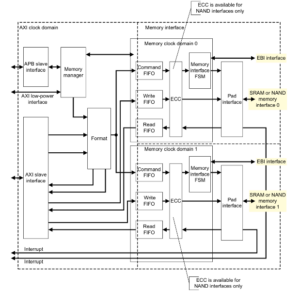
SMC diagram from the TRM

The SMC can interface with two different memory types: NAND or SRAM/NOR. As it features two memory slots, this means that it can drive two memories, but they must be of the same type. When handling NAND devices, a hardware ECC engine is available to perform on-the-fly correction.

As only a single type of memory device can be plugged in at a time (either two SRAM/NORs or two NANDs), we don’t need to share a lot of controls with the SRAM/NOR controllers. So in the end the memory bus driver is almost an empty envelope that relies on the child controller driver to do the job.

Interactions with a memory device

On the CPU side, the controller has two main interfaces: APB and AXI.

The APB interface works like any regular interface: the CPU sees registers that it can access with diverse read and write operations, which will effectively read and write the content of the 32-bit registers located at the desired addresses. This is how the driver configures the device type, the timings, the possible ECC configuration and so forth. All the initial SMC configuration is done through the APB interface.

The AXI interface does not quite work like this. Instead of featuring a set of registers at a fixed address in which the content of the command, address and data cycles would be written in order to be forwarded to the memory device, the AXI interface needs to reserve a notable range in the addressable space. In particular, the offset targetted by the AXI write depend on the type of action that must be performed and the content of the action:

  • When requesting the controller to send command and address cycles to the memory device, the datasheet refers to it as the “command phase”.
  • When doing I/Os, eg. actually reading from/writing to the memory device, the datasheet calls this the “data phase”.

Both the command and data phase use regular AXI read/writes, but the offsets and values are different than usual.

Command phase

When the driver wants to send command cycles, it must perform one or two register writes. The address of the write operation in the AXI address space must target a specific offset. This offset indicates a number of information:

  • A specific bit is set to tell the SMC that it must enter a command phase.
  • Part of the offset are made of the shifted values of the different command opcodes for the memory device.
  • Part of the offset encodes the number of address cycles to perform on the NAND bus.

The payload of the AXI write contains the value of the address cycles that should be forwarded to the memory device. If there are more than 4 address cycles (which is quite common today), then a second AXI write containing the remaining address cycles as payload must happen at the same offset as before.

/*
 * Define the offset in the AXI address space where to write with:
 * - the bit indicating the command phase
 * - the number of address cycles
 * - the command opcode
 */
cmd_addr = PL35X_SMC_CMD_PHASE |
           PL35X_SMC_CMD_PHASE_NADDRS(naddr_cycles) |
           PL35X_SMC_CMD_PHASE_CMD0(NAND_CMD_XXXX);

/* Define the payload with the address bytes */
for (i = 0, row = 0; row < nrows; i++, row++) {
        [...]
        if (row < 4)
                addr1 |= PL35X_SMC_CMD_PHASE_ADDR(row, addr);
        else
                addr2 |= PL35X_SMC_CMD_PHASE_ADDR(row - 4, addr);
}

/* Send the command and address cycles */
writel(addr1, nfc->io_regs + cmd_addr);
if (naddr_cycles > 4)
        writel(addr2, nfc->io_regs + cmd_addr);

Data phase

The data phase is a bit easier to understand: several AXI reads or writes will be performed at a specific offset. The payload matches our expectations: it is actually the data that we want to read from or write to the device. However, the offset in the AXI address space is again a bit counter-intuitive:

  • It contains a specific bit such as the command phase to inform the controller that the data phase must be entered.
  • It also contains shifted values of different flags regarding the ECC configuration. The thing is, this offset will change at the end of the I/O operation because the last chunk of data must always be handled differently because of the ECC calculations that must be manually started. We end up reading or writing physically contiguous data by accessing two completely different offsets.
/* I/O transfers: simple case */
for (i = 0; i < buf_end; i++) {
        data_phase_addr = PL35X_SMC_DATA_PHASE;
        if (i + 1 == buf_end)
                data_phase_addr += PL35X_SMC_DATA_PHASE_ECC_LAST;

        writel(buf32[i], nfc->io_regs + data_phase_addr);
}

But what happens if a command cycle must be sent at the end of a data transfer (typical case of a PAGE_WRITE)? While it would certainly be more logical to perform an additional command phase AXI write, it was certainly more optimized to merge data and command phase on the last access. And here is how it looks like:

/* I/O transfers: less straightforward situation */
for (i = 0; i < buf_end; i++) {
        data_phase_addr = PL35X_SMC_DATA_PHASE;
        if (i + 1 == buf_end)
                data_phase_addr +=
                    PL35X_SMC_DATA_PHASE_ECC_LAST |
                    PL35X_SMC_CMD_PHASE_CMD1(NAND_CMD_PAGEPROG) |
                    PL35X_SMC_CMD_PHASE_CMD1_VALID);

        writel(buf32[i], nfc->io_regs + data_phase_addr);
}

Of course, nothing highly unreadable, but at the very least, these accesses are quite uncommon.

A memory bus driver and a NAND controller driver

As explained earlier, this SMC controller can support different types of memories, and this has called for a Device Tree representation where the SMC controller is one node, and the memories connected to it are represented as sub-node. So, the Device Tree representation of the SMC controller, used with its NAND controller looks like this:

    smcc: memory-controller@e000e000 {
      compatible = "arm,pl353-smc-r2p1", "arm,primecell";
      reg = <0xe000e000 0x0001000>;
      clock-names = "memclk", "apb_pclk";
      clocks = <&clkc 11>, <&clkc 44>;
      ranges = <0x0 0x0 0xe1000000 0x1000000 /* Nand CS region */
                0x1 0x0 0xe2000000 0x2000000 /* SRAM/NOR CS0 region */
                0x2 0x0 0xe4000000 0x2000000>; /* SRAM/NOR CS1 region */
      #address-cells = <2>;
      #size-cells = <1>;

      nfc0: nand-controller@0,0 {
        compatible = "arm,pl353-nand-r2p1";
        reg = <0 0 0x1000000>;
        #address-cells = <1>;
        #size-cells = <0>;
      };
    };

So, we first have a node for the SMC controller itself, memory-controller@e000e000, which will allow probing the memory bus driver located at drivers/memory/pl353-smc.c. This driver is very simple: it enables the clocks necessary for the SMC to work, and then it probes the first child device that matches either the cfi-flash or arm,pl353-nand-r2p1 compatible strings. In the latter case (which is illustrated in our example), the NAND controller driver at drivers/mtd/nand/raw/pl35x-nand-controller.c will be probed, and where the two memory areas (accessed through APB and AXI) will be mapped, and accessed to program the NAND controller.

Now in the mainline Linux kernel

Starting from the latest version posted by Xilinx, Miquèl Raynal, Bootlin’s NAND/MTD expert, performed a massive cleanup of the memory bus driver and the NAND controller driver, rewrote entirely the binding file (in YAML schema!) and three versions later, with the support of Xilinx engineers and the acknowledgements of Rob Herring and Krzysztof Kozlowski, managed to finally close the story. The driver is now part of Linux 5.14-rc, and will therefore be in the final Linux 5.14 release in a few weeks!

Bringing NV-DDR support to parallel NAND flashes in Linux

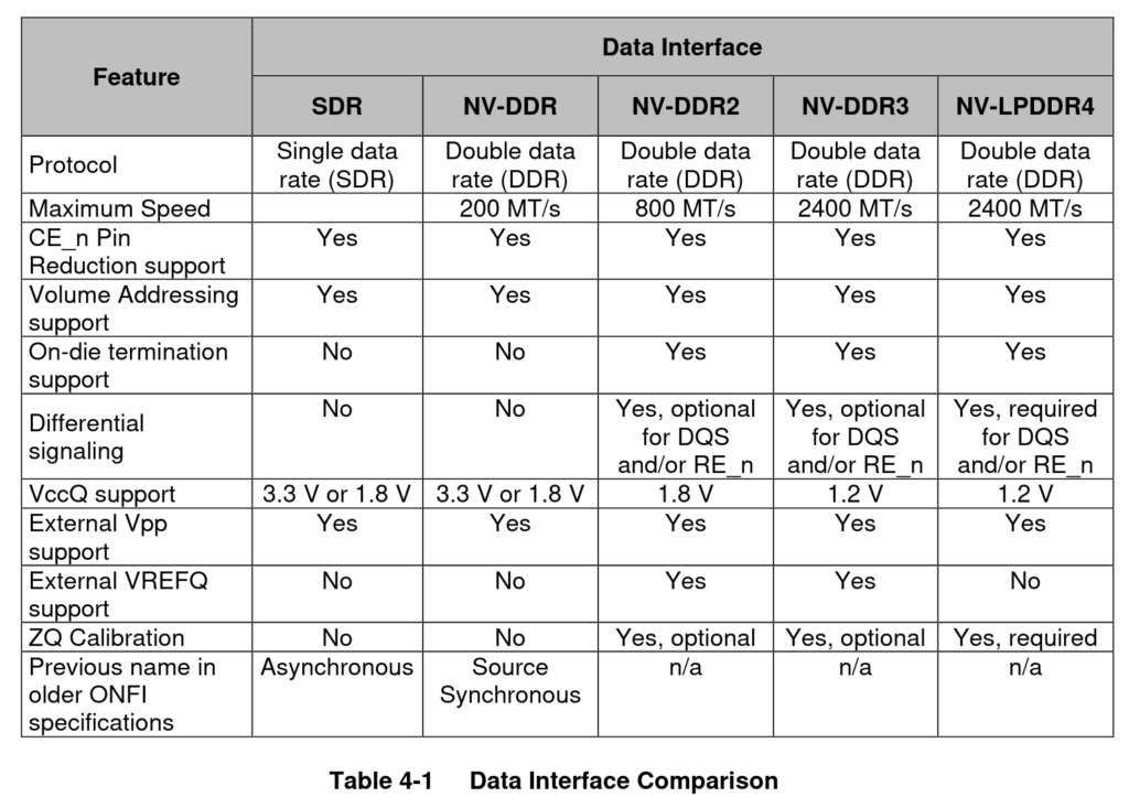
We have recently contributed support for NV-DDR interfaces to parallel NAND flashes in the Linux kernel, which brings performance improvements for a number of NAND flash devices. In this article, we will detail what are the ONFI specifications, the historical SDR interface, then the introduction of faster interfaces in the ONFI specification, and finally our work to support such interfaces in the Linux kernel.

ONFI specifications

Even though specifications came after the introduction of NAND devices on the market, the Open NAND Flash Interface (ONFI) specification is nowadays a de-facto specification which many NAND chip support (even non-ONFI ones). For instance, in the Linux kernel, we assume that any NAND flash device will by default, after a reset command, at least support the slowest set of ONFI timings. Other specifications exist, like the Joint Electron Device Engineering Council (JEDEC), but as it is a bit less common in the parallel NAND flashes world, we will focus on the ONFI details in this blog post.

The early days of the SDR interface

At the time of the first ONFI specification back in 2006, there was only a single interface detailed: the asynchronous data interface. Also known as Single Data Rate or SDR interface in modern language, it defines the timings sequence that should be respected in order for any NAND controller to be able to deal with almost any kind of NAND device. As an asynchronous interface, in this interface, the data bus has no clock signal. Instead, it features a specific set of signals which are asserted by the controller to signal read data latch and write data latch: Read Enable (RE#) and Write Enable (WE#).

The data interface can work in 6 different timing modes, from 0 to 5. 0 is the slowest mode and the default one at boot time with a theoretical data rate of about 10MiB/s (assuming an 8-bit bus). Mode 4 and 5 are the fastest, they leverage the ability of Extended Data Output (EDO) to latch data on both RE#/WE# edges and may reach a theoretical data rate of 50MiB/s.

The introduction of faster interfaces

Shortly after, at the beginning of 2008, the ONFI consortium released the second version of the ONFI specification and included a new interface: the source synchronous data interface. This interface is backward compatible with the asynchronous interface and allows the host to switch from one interface to the other if this is needed. In the particular case of the source synchronous interface, a clock (CLK) signal is replacing the legacy WE# signal and indicates when the commands and address should be latched. The direction of the transfers is handled by the Write/Read signal (W/R#) in place of RE# signal. Finally, a data strobe (DQS) signal is being introduced and indicates when the data should be latched. As both edges of the DQS signal advertise for a data latch, the source synchronous interface is also called Double Data Rate (DDR) interface even though this naming was only introduced in the version 3.0 of the specification, in 2011.

The exact terms that are used in more recent specifications are NV-DDR (Non-Volatile DDR), NV-DDR2 and NV-DDR3 which are backward compatible improvements of the NV-DDR interface. For instance, the first NV-DDR specification has a range of theoretical rates from 40MiB/s to 200MiB/s.

ONFI datasheet on data interfaces

Support in the Linux kernel

While the addition of the MTD/NAND subsystem in the Linux kernel predates the Git era and is now over 20 years old, Linux users have always been limited to use the asynchronous interface (SDR modes). At Bootlin, we recently started an effort to bring support for the NV-DDR interface to the Linux kernel MTD/NAND subsystem, and this involved the following changes:

  • Introducing an API to propose timings to the host controller driver, so that it might either accept or refuse them (only SDR mode 0 cannot be refused) and be aware of all timings that this choice involves so that the host controller registers will be configured properly.
  • Adding the possibility for NAND chip drivers to tweak the timings if the parameter page is not present or inaccurate.
  • Adding the core logic to ask the NAND chip to change its data interface through the use of GET_FEATURE and SET_FEATURE calls, as well as verifying that this operation worked correctly and handling the fallback in case of error.

We recently reached a final step in this effort as the last missing parts will be part of the next Linux kernel release (v5.14). This final series aiming at bringing NV-DDR support to Linux carries the following changes:

  • Adding the necessary bits to parse the parameter page of the NAND device in order to know which NV-DDR modes the chips support.
  • Providing the reference implementation of all NV-DDR timing modes and various helpers to manage them.
  • Adding the necessary infrastructure and helpers to the host controller drivers in order to allow them to distinguish between SDR and NV-DDR, as well as advertise which mode they are willing to support based on the controller’s constraints.
  • Updating the existing logic to take into account the existence of NV-DDR timings and select them when appropriate. This part is a bit trickier as the core must gracefully fallback to SDR modes under certain conditions.

Overall, thanks to the major cleanups which happened in the NAND subsystem in the last three years, it was pretty straightforward to add support for these new timings.

Future work

It is worth mentioning that accelerating the overall throughput on the data bus without a deeper rework of the MTD core than just enabling faster timings is very limiting: data reads must respect a tR delay before starting and writes are considered effective only after a tPROG delay. Both are significantly high in practice: respectively about 25-45us and 200-600us, compared to the time needed to store/fetch the data through the I/O bus: a few dozens of micro-seconds.

To fully leverage the power of NV-DDR timings the NAND and MTD cores should be partially rewritten to bring parallel multi-die support and cached operations. Such features would allow to optimize the use of the I/O bus in order to mitigate the performances impact of tR and tPROG during massive I/O operations. This is precisely one of the tricks used by SSD drives to exhibit very fast I/Os while using multiple NAND chips behind. There is therefore interesting additional work to do in the Linux kernel MTD subsystem to fully benefit from NV-DDR interfaces.

Supporting a misbehaving NAND ECC engine

Over the years, Bootlin has grown a significant expertise in U-Boot and Linux support for flash memory devices. Thanks to this expertise, we have recently been in charge of rewriting and upstreaming a driver for the Arasan NAND controller, which is used in a number of Xilinx Zynq SoCs. It turned out that supporting this NAND controller had some interesting challenges to handle its ECC engine peculiarities. In this blog post, we would like to give some background about ECC issues with NAND flash devices, and then dive into the specific issues that we encountered with the Arasan NAND controller, and how we solved them.

Ensuring data integrity

NAND flash memories are known to be intrinsically rather unstable: over time, external conditions or repetitive access to a NAND device may result in the data being corrupted. This is particularly true with newer chips, where the number of corruptions usually increases with density, requiring even stronger corrections. To mitigate this, Error Correcting Codes are typically used to detect and correct such corruptions, and since the calculations related to ECC detection and correction are quite intensive, NAND controllers often embed a dedicated engine, the ECC engine, to offload those operations from the CPU.

An ECC engine typically acts as a DMA master, moving, correcting data and calculating syndromes on the fly between the controller FIFO’s and the user buffer. The engine correction is characterized by two inputs: the size of the data chunks on which the correction applies and the strength of the correction. Old SLC (Single Level Cell) NAND chips typically require a strength of 1 symbol over 4096 (1 bit/512 bytes) while new ones may require much more: 8, 16 or even 24 symbols.

In the write path, the ECC engine reads a user buffer and computes a code for each chunk of data. NAND pages being longer than officially advertised, there is a persistent Out-Of-Band (OOB) area which may be used to store these codes. When reading data, the ECC engine gets fed by the data coming from the NAND bus, including the OOB area. Chunk by chunk, the engine will do some math and correct the data if needed, and then report the number of corrected symbols. If the number of error is higher than the chosen strength, the engine is not capable of any correction and returns an error.

The Arasan ECC engine

As explained in our introduction, as part of our work on upstreaming the Arasan NAND controller driver, we discovered that this NAND controller IP has a specific behavior in terms of how it reports ECC results: the hardware ECC engine never reports errors. It means the data may be corrected or uncorrectable: the engine behaves the same. From a software point of view, this is a critical flaw and fully relying on such hardware was not an option.

To overcome this limitation, we investigated different solutions, which we detail in the sections below.

Suppose there will never be any uncorrectable error

Let’s be honest, this hypothesis is highly unreliable. Besides that anyway, it would imply that we do not differentiate between written/erased pages and users would receive unclean buffers (with bitflips), which would not work with upper layers such as UBI/UBIFS which expect clean data.

Keep an history of bitflips of every page

This way, during a read, it would be possible to compare the evolution of the number of bitflips. If it suddenly drops significantly, the engine is lying and we are facing an error. Unfortunately it is not a reliable solution either because we should either trigger a write operation every time a read happens (slowing down a lot the I/Os and wearing out very quickly the storage device) or loose the tracking after every power cycle which would make this solution very fragile.

Add a CRC16

This CRC16 could lay in the OOB area and help to manually verify the data integrity after the engine’s correction by checking it against the checksum. This could be acceptable, even if not perfect in term of collisions. However, it would not work with existing data while there are many downstreams users of the vendor driver already.

Use a bitwise XOR between raw and corrected data

By doing a bitwise XOR between raw and corrected datra, and compare with the number of bitflips reported by the engine, we could detect if the engine is lying on the number of corrected bitflips. This solution has actually been implemented and tested. It involves extra I/Os as the page must be read twice: first with correction and then again without correction. Hence, the NAND bus throughput becomes a limiting factor. In addition, when there are too many bitflips, the engine still tries to correct data and creates bitflips by itself. The result is that, with just a XOR, we cannot discriminate a working correction from a failure. The following figure shows the issue.
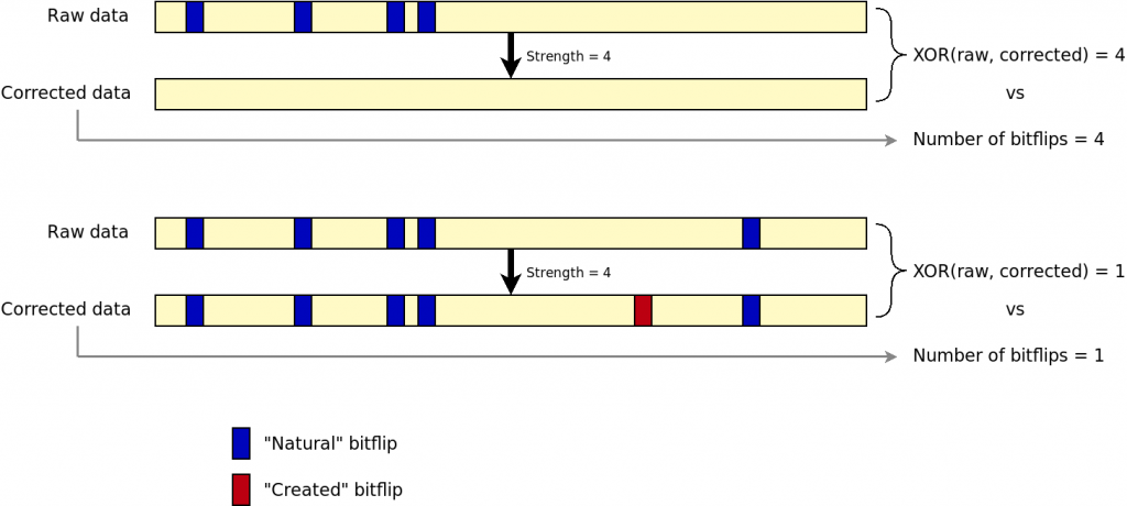
Show the engine issue when it creates bitflips when trying to correct uncorrectable data

Rely on the hardware only in the write path

Using the hardware engine in the write path is fine (and possibly the quickest solution). Instead of trying to workaround the flaws of the read path, we can do the math by software to derive the syndrome in the read path and compare it with the one in the OOB section. If it does not match, it means we are facing an uncorrectable error. This is finally the solution that we have chosen. Of course, if we want to compare software and hardware calculated ECC bytes, we must find a way to reproduce the hardware calculations, and this is what we are going to explore in the next sections.

Reversing a hardware BCH ECC engine

There is already a BCH library in the Linux kernel on which we could rely on to compute BCH codes. What needed to be identified though, were the BCH initial parameters. In particular:

  • The BCH primary polynomial, from which is derived the generator polynomial. The latter is then used for the computation of BCH codes.
  • The range of data on which the derivation would apply.

There are several thousands possible primary polynomials with a form like x^3 + x^2 + 1. In order to represent these polynomials more easily by software, we use integers or binary arrays. In both cases, each bit represents the coefficient for the order of magnitude corresponding to its position. The above example could be represented by b1101 or 0xD.

For a given desired BCH code (ie. the ECC chunk size and hence its corresponding Gallois Field order), there is a limited range of possible primary polynomials which can be used. Given eccsize being the amount of data to protect, the Gallois Field order is the smallest integer m so that: 2^m > eccsize. Knowing m, one can check these tables to see examples of polynomials which could match (non exhaustive). The Arasan ECC engine supporting two possible ECC chunk sizes of 512 and 1024 bytes, we had to look at the tables for m = 13 and m = 14.

Given the required strength t, the number of needed parity bits p is: p = t x m.

The total amount of manipulated data (ECC chunk, parity bits, eventual padding) n, also called BCH codeword in papers, is: n = 2^m - 1.

Given the size of the codeword n and the number of parity bits p, it is then possible to derive the maximum message length k with: k = n - p.

The theory of BCH also shows that if (n, k) is a valid BCH code, then (n - x, k - x) will also be valid. In our situation this is very interesting. Indeed, we want to protect eccsize number of symbols, but we currently cover k within n. In other words we could use the translation factor x being: x = k - eccsize. If the ECC engine was also protecting some part of the OOB area, x should have been extended a little bit to match the extra range.

With all this theory in mind, we used GNU Octave to brute force the BCH polynomials used by the Arasan ECC engine with the following logic:

  • Write a NAND page with a eccsize-long ECC step full of zeros, and another one full of ones: this is our known set of inputs.
  • Extract each BCH code of p bits produced by the hardware: this is our known set of outputs.

For each possible primary polynomial with the Gallois Field order m, we derive a generator polynomial, use it to encode both input buffers thanks to a regular BCH derivation, and compare the output syndromes with the expected output buffers.

Because the GNU Octave program was not tricky to write, we first tried to match with the output of Linux software BCH engine. Linux using by default the primary polynomial which is the first in GNU Octave’s list for the desired field order, it was quite easy to verify the algorithm worked.

As unfortunate as it sounds, running this test with the hardware data did not gave any match. Looking more in depth, we realized that visually, there was something like a matching pattern between the output of the Arasan engine and the output of Linux software BCH engine. In fact, both syndromes where identical, the bits being swapped at byte level by the hardware. This observation was made possible because the input buffers have the same values no matter the bit ordering. By extension, we also figured that swapping the bits in the input buffer was also necessary.

The primary polynomial for an eccsize of 512 bytes being already found, we ran again the program with eccsize being 1024 bytes:

eccsize = 1024
eccstrength = 24
m = 14
n = 16383
p = 336
k = 16047
x = 7855
Trying primary polynomial #1: 0x402b
Trying primary polynomial #2: 0x4039
Trying primary polynomial #3: 0x4053
Trying primary polynomial #4: 0x405f
Trying primary polynomial #5: 0x407b
[...]
Trying primary polynomial #44: 0x43c9
Trying primary polynomial #45: 0x43eb
Trying primary polynomial #46: 0x43ed
Trying primary polynomial #47: 0x440b
Trying primary polynomial #48: 0x4443
Primary polynomial found! 0x4443

Final solution

With the two possible primary polynomials in hand, we could finish the support for this ECC engine.

At first, we tried a “mixed-mode” solution: read and correct the data with the hardware engine and then re-read the data in raw mode. Calculate the syndrome over the raw data, derive the number of roots of the syndrome which represents the number of bitflips and compare with the hardware engine’s output. As finding the syndrome’s roots location (ie. the bitflips offsets) is very time consuming for the machine it was decided not to do it in order to gain some time. This approach worked, but doing the I/Os twice was slowing down very much the read speed, much more than expected.

The final approach has been to actually get rid of any hardware computation in the read path, delegating all the work to Linux BCH logic, which indeed worked noticeably faster.

The overall work is now in the upstream Linux kernel:

If you’re interested about more details on ECC for flash devices, and their support in Linux, we will be giving a talk precisely on this topic at the upcoming Embedded Linux Conference!

Bootlin adds SPI NAND support to U-Boot


Bootlin is proud to announce that it has contributed SPI NAND support to the U-Boot bootloader, which is part of the recently released U-Boot 2018.11. Thanks to this effort, one can now use SPI NAND memories from U-Boot, a feature that had been missing for a long time.

State of the art: Linux support

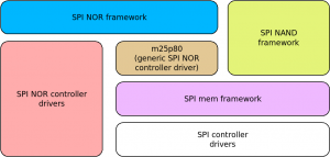
A few months ago, Bootlin engineer Boris Brezillon added SPI-NAND support in the Linux kernel, based on an initial contribution from Peter Pan. As Boris explained in a previous blog post, adding SPI NAND support in Linux required adding a new spi-mem layer, that allows SPI NOR and SPI NAND drivers to leverage regular SPI controller drivers, but also to allow those SPI controller drivers to expose optimized operations for flash memory access. The spi-mem layer was added to the SPI subsystem by a first series of patches, while the SPI NAND support itself was added to the MTD subsystem as part of another patch series.

The spi-mem framework in Linux

Moving to U-Boot

Since accessing flash memories from the bootloader is often necessary, Bootlin engineer Miquèl Raynal took the challenge of adding SPI NAND support in U-Boot. Miquèl did this by porting the SPI-mem and SPI-NAND subsystems from Linux to U-Boot. The first challenge when porting the SPI-mem and SPI-NAND code from Linux to U-Boot was that the U-Boot MTD stack hadn’t been synchronized with the one of Linux for quite some time. Thus a number of changes in the Linux MTD subsystem had to be ported to U-Boot as well, which was a fairly time-consuming effort. The SPI NAND code has been imported in drivers/mtd/nand/spi, while the spi-mem layer is in drivers/spi/spi-mem.c.

Once the core code was ready, we had to find a way to let the user interact with the SPI NAND devices. Until now, U-Boot had a separate set of commands for each type of flash memory (nand for parallel NAND, erase/cp for parallel NOR, sf for SPI NOR), and it indeed seemed like adding yet another command was the way to go. Instead, we introduced a new mtd that can be used to access all flash memory devices, regardless of their specific type. We will discuss this mtd in more details in another blog post.

However, such a move to a generic mtd command forced us to do a lot more cleanup than expected, as we ended up reworking the MTD partition handling, and even making deep changes in the ubi command. This was more complicated than anticipated because of the SPI NOR support in U-Boot: it is not very well integrated with MTD subsystem, in the sense that there is a duplication of information between the SPI NOR and MTD subsystems, and when the duplicated information is no longer consistent, really bad things happen. As an example, any call to sf probe was doing a reset of the MTD device structure using memset, causing all other state information contained in this structure to be lost. Since the SPI NAND support relies on the MTD subsystem (much more than the current SPI NOR support), we had to mitigate those issues. Long term, a proper rework of the SPI NOR support in U-Boot is definitely needed.

Some of those issues are present in the 2018.11 release and were discovered by U-Boot users who started testing the new mtd command. We have contributed a patch series addressing them, which hopefully should be merged soon.

Now that those difficulties are hopefully behind us, the U-Boot SPI-NAND support looks pretty stable, and we have quite a few SPI-NAND manufacturer drivers in U-Boot mainline, with Gigadevice, Macronix, Micron and Winbond supported so far. We’re happy to have contributed this new significant feature, as it finally allows to use this popular type of flash memory in U-Boot.

Bootlin contributes a new interface to the Linux NAND subsystem

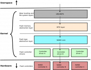
MTD stack

Over the last months, Bootlin engineers Boris Brezillon and Miquèl Raynal have been working on rewriting the NAND controller driver used on a large number of Marvell SoCs. This NAND controller driver had grown very complicated, and Miquèl’s adventure in this rework led him to contribute a new interface to the NAND framework, in order to simplify implementing NAND controller drivers for complex NAND controllers. In this blog post, Miquèl summarizes the original issue, and how it is solved by the ->exec_op() interface he has contributed.

Introduction

The NAND framework is the layer between the generic MTD layer and the NAND controller drivers. Its purpose is to handle MTD requests and transform them into understandable NAND operations the controller will have to send to the NAND chip.

For general information about NANDs, the reader is invited to read the ONFI specification (Open NAND Flash Interface) which defines the most common NAND operations.

Interacting with a NAND chip

Raw NANDs (so-called “parallel NANDs”) are slave devices waiting for instructions from the controller. An operation is a sequence of instructions usually referred as “command” (CMD), “addresses” (ADDR), and “data” cycles (DATA_IN/DATA_OUT) and sometimes wait periods (WAITRDY). Some everyday operations any NAND enthusiast should know by heart are, for instance:

NAND operation example

How it was handled in the Linux kernel

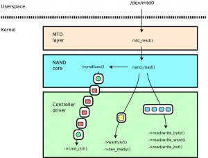
Today, a majority of NAND controlller drivers implement the ->cmd_ctrl() hook. It aimed to be a very small function, designed to just send command and address cycles independently, usually embedding some very controller-specific logic. This hook was supposed to be called by a function of higher level from the NAND core, ->cmdfunc(). In addition to calling ->cmd_ctrl() to send command and address cycles, the core would also call ->read|write_byte|word|buf() hooks to actually move data from the NAND controller and the memory (the DATA parts in the diagram above).

This approach worked very well with simple NAND controllers, which are just able to send command and address cycles one at a time to the NAND chip, without any extra intelligence. However, NAND controllers have become more and more complex and now can handle higher-level operations, usually to provide higher performance. For example, a NAND controller may provide an operation that would do all of the command and address cycles of a read-page operation in one-go. Some controllers even support only those higher-level operations, and are not able to simply do the basic operation of sending one command cycle or one data cycle. To handle such controllers, their drivers were overloading the ->cmdfunc() hook directly, circumventing the generic NAND core implementation of ->cmdfunc(). This is a first drawback: it is no longer possible to easily add logic to the NAND core to support new NAND operations, because some drivers overload the ->cmdfunc() logic. Worse, ->cmdfunc() doesn’t provide some information such as the length of the data transfer, which some controllers actually need in order to run the desired operation. NAND controller drivers started to have complicated state machines just to work around the NAND framework limitations.

NAND stack before exec_op

Some driver-specific implementations of this hook started diverging from the original one, giving maintainers a lot of pain to maintain the whole subsystem, specifically when they needed to introduce additional vendor-specific operations support. These implementations were not only diverse but also incomplete, sometimes buggy and most importantly, developers had to guess the data that would probably be moved by the core after that, which is clearly a symptom that the framework was not fitting the user needs anymore.

The ->exec_op() era

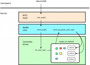
The NAND subsystem maintainers decided to switch to a new approach, based on a new hook called ->exec_op(), implemented by NAND controller drivers and called by the generic NAND core. The logic behind that name is to provide to every controller a generic interface that can easily be extended and exposes the overall NAND operation to be performed. This way, the driver can optimize depending on the controller capabilities without the need of a complex state machine as ->cmdfunc() was.

All major NAND generic raw operations like reset, reading the NAND ID, selecting a set of timings, reading/writing data and so on found their place into small internal functions named nand_[operation]_op().

From the NAND controller driver point of view, an array of instructions is received for each operation. The controller then needs to parse these instructions, decides if it can handle the overall operation, splits the operation if needed, and executes what is requested.

Using the ->exec_op() interface is as simple as declaring a list with the controller capabilities, each entry of this array having a callback function knowing the overall operation that will actually handle all the logic. The NAND core was enhanced with a proper parser that one may use in his driver to handle the callback selection logic.

NAND stack with exec_op

For a more complete overview, one can check the slides and the video of Miquèl’s presentation at FOSDEM about NAND flash memories and the introduction of ->exec_op() in the Linux kernel.

Current status

The ->exec_op() interface in the NAND core has been accepted and merged upstream, and will be part of Linux 4.16. The first driver converted to this new interface was obviously the NAND controller driver used on Marvell platforms, pxa3xx_nand. It has been rewritten as marvell_nand, and will also be part of Linux 4.16. Even though the new driver is longer (by lines of code) than the previous one, it supports additional features (such as raw read and write operations), allows the NAND core to pass custom commands to the NAND chip, and has a logic that is a lot less complicated.

Miquèl has also worked on converting the fsmc_nand driver to ->exec_op(), but this work hasn’t been merged yet. In the community, Stefan Agner has taken on the task to convert the vf610_nfc driver to this new approach.

Bootlin is proud to have contributed such enhancements to the Linux kernel, and hopes to see other developers contribute to this subsystem in the near future, by migrating their favorite NAND controller driver to ->exec_op()!

Linux 4.9 released, Bootlin contributions

Linus Torvalds has released the 4.9 Linux kernel yesterday, as was expected. With 16214 non-merge commits, this is by far the busiest kernel development cycle ever, but in large part due to the merging of thousands of commits to add support for Greybus. LWN has very well summarized what’s new in this kernel release: 4.9 Merge window part 1, 4.9 Merge window part 2, The end of the 4.9 merge window.

As usual, we take this opportunity to look at the contributions Bootlin made to this kernel release. In total, we contributed 116 non-merge commits. Our most significant contributions this time have been:

  • Bootlin engineer Boris Brezillon, already a maintainer of the Linux kernel NAND subsystem, becomes a co-maintainer of the overall MTD subsystem.
  • Contribution of an input ADC resistor ladder driver, written by Alexandre Belloni. As explained in the commit log: common way of multiplexing buttons on a single input in cheap devices is to use a resistor ladder on an ADC. This driver supports that configuration by polling an ADC channel provided by IIO.
  • On Atmel platforms, improvements to clock handling, bug fix in the Atmel HLCDC display controller driver.
  • On Marvell EBU platforms
    • Addition of clock drivers for the Marvell Armada 3700 (Cortex-A53 based), by Grégory Clement
    • Several bug fixes and improvements to the Marvell CESA driver, for the crypto engine founds in most Marvell EBU processors. By Romain Perier and Thomas Petazzoni
    • Support for the PIC interrupt controller, used on the Marvell Armada 7K/8K SoCs, currently used for the PMU (Performance Monitoring Unit). By Thomas Petazzoni.
    • Enabling of Armada 8K devices, with support for the slave CP110 and the first Armada 8040 development board. By Thomas Petazzoni.
  • On Allwinner platforms
    • Addition of GPIO support to the AXP209 driver, which is used to control the PMIC used on most Allwinner designs. Done by Maxime Ripard.
    • Initial support for the Nextthing GR8 SoC. By Mylène Josserand and Maxime Ripard (pinctrl driver and Device Tree)
    • The improved sunxi-ng clock code, introduced in Linux 4.8, is now used for Allwinner A23 and A33. Done by Maxime Ripard.
    • Add support for the Allwinner A33 display controller, by re-using and extending the existing sun4i DRM/KMS driver. Done by Maxime Ripard.
    • Addition of bridge support in the sun4i DRM/KMS driver, as well as the code for a RGB to VGA bridge, used by the C.H.I.P VGA expansion board. By Maxime Ripard.
  • Numerous cleanups and improvements commits in the UBI subsystem, in preparation for merging the support for Multi-Level Cells NAND, from Boris Brezillon.
  • Improvements in the MTD subsystem, by Boris Brezillon:
    • Addition of mtd_pairing_scheme, a mechanism which allows to express the pairing of NAND pages in Multi-Level Cells NANDs.
    • Improvements in the selection of NAND timings.

In addition, a number of Bootlin engineers are also maintainers in the Linux kernel, so they review and merge patches from other developers, and send pull requests to other maintainers to get those patches integrated. This lead to the following activity:

  • Maxime Ripard, as the Allwinner co-maintainer, merged 78 patches from other developers.
  • Grégory Clement, as the Marvell EBU co-maintainer, merged 43 patches from other developers.
  • Alexandre Belloni, as the RTC maintainer and Atmel co-maintainer, merged 26 patches from other developers.
  • Boris Brezillon, as the MTD NAND maintainer, merged 24 patches from other developers.

The complete list of our contributions to this kernel release:

Bootlin engineer Boris Brezillon becomes Linux NAND subsystem maintainer

Bootlin engineer Boris Brezillon has been involved in the support for NAND flashes in the Linux kernel for quite some time. He is the author of the NAND driver for the Allwinner ARM processors, did several improvements to the NAND GPMI controller driver, has initiated a significant rework of the NAND subsystem, and is working on supporting MLC NANDs. Boris is also very active on the linux-mtd mailing list by reviewing patches from others, and making suggestions.

Hynix NAND flash

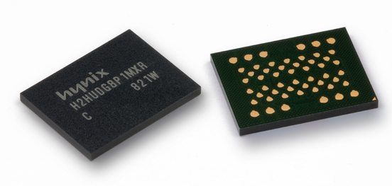
For those reasons, Boris was recently appointed by the MTD maintainer Brian Norris as a new maintainer of the NAND subsystem. NAND is considered a sub-subsystem of the MTD subsystem, and as such, Boris will be sending pull requests to Brian, who in turn is sending pull requests to Linus Torvalds. See this commit for the addition of Boris as a NAND maintainer in the MAINTAINERS file. Boris will therefore be in charge of reviewing and merging all the patches touching drivers/mtd/nand/, which consist mainly of NAND drivers. Boris has created a nand/next branch on Github, where he has already merged a number of patches that will be pushed to Brian Norris during the 4.7 merge window.

We are happy to see one of our engineers taking another position as a maintainer in the kernel community. Maxime Ripard was already a co-maintainer of the Allwinner ARM platform support, Alexandre Belloni a co-maintainer of the RTC subsystem and Atmel ARM platform support, Grégory Clement a co-maintainer of the Marvell EBU platform support, and Antoine Ténart a co-maintainer of the Annapurna Labs platform support.