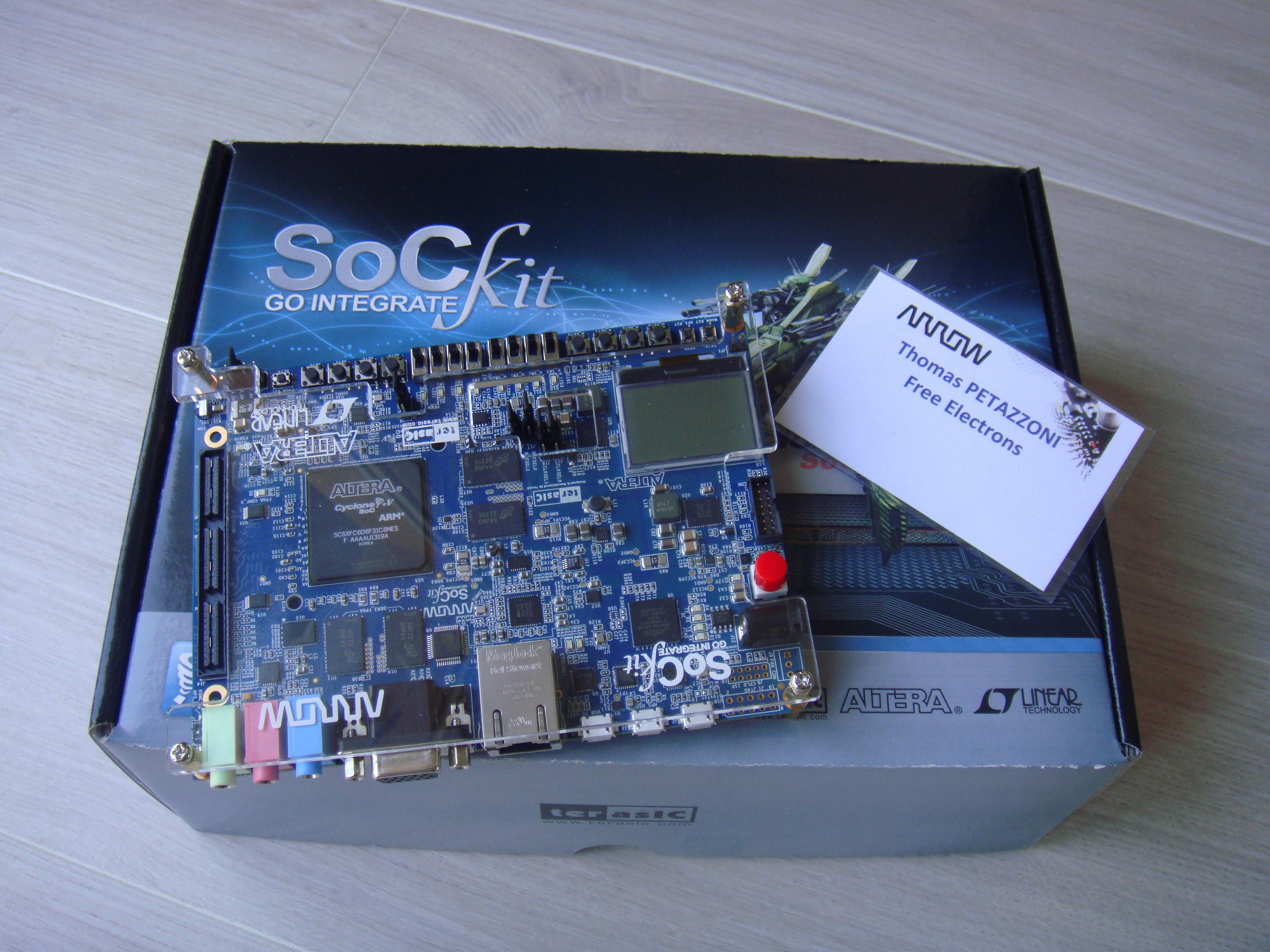
On June 25, 2013, Altera and some partner companies where organizing a workshop in Toulouse (where some of the Bootlin offices are located) about the Altera SoC FPGA platform. For $99, I participated to this full-day workshop, with a small training of the hardware and software tools available for this platform, and went away with a the development kit that was used for the practical labs, the Arrow SoCKit evaluation board.
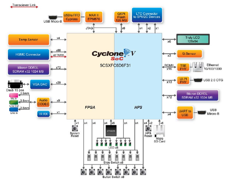
The Altera SoC FPGA platform is a single chip that combines a dual Cortex-A9 processor and a Cyclone V FPGA (other variants are available, such as single core ARM, or bigger FPGAs). Since both are integrated on the same chip, it removes the need for a complex bus between the application processor and a separate FPGA, and it provides a very high bandwidth between the processor and the FPGA to exchange data. As can be seen on the following diagram, the Arrow SocKit evaluation board has a good number of peripherals, some of them connected to the HPS side of the processor (HPS stands for Hard Processor System, which is dual Cortex-A9 and all the hard peripherals), and some others connected to the FPGA side of the processor. Specifically, the workshop was centered around playing with the LEDs and the buttons connected to the FPGA side.

The morning of the workshop was dedicated to the hardware part, using two tools: Qsys (Altera’s System Integration Tool) and Quartus II (FPGA design). The Qsys tool allows to graphically build the hardware architecture of the SoC FPGA: you can bring the Hard Processor System, and then some additional FPGA IPs and connect them together. In the examples, two PIO IPs were added to the FPGA side, one to control LEDs and the other to control buttons. All the pin muxing and the DRAM configuration also takes place in Qsys, which in the end will automatically generate numerous elements:
- FPGA code to be used by Quartus (for the FPGA side)
- pre-loader source code (actually modifications to U-Boot to take into account the pin muxing and the DRAM configuration)
- a Device Tree for the Linux kernel (that takes into account all the peripherals enabled in the system configuration)
- etc.

Once this system-level configuration is done with Qsys, Quartus is used to synthesize the FPGA side. Finally, the FPGA bitstream can be loaded into the FPGA, and using a JTAG connection and a System Console tool, one can directly read/write the registers of the FPGA IPs that have been integrated, and easily test them without having any software running. With the SOCKit evaluation board, the JTAG connection takes place through a USB to micro-USB cable, so no special hardware is needed.
The afternoon of the workshop was dedicated to the software part, obviously mostly centered on U-Boot and Linux. The pre-loader source code (actually the U-Boot SPL) is generated by the Qsys tool to take into account all the details of the system configuration, so after doing a build of U-Boot, the labs explained how to push the U-Boot binary to the board using the JTAG connection, under the DS-5 development environment (which is the development environment provided by ARM, based on Eclipse, with a special integration of Altera tools). The lab showed that you can set breakpoints, and do step by step execution of U-Boot, as one would expect. One nice thing is that the “Peripheral Registers” view in DS-5 is automatically updated according to the hardware components in the system: all the registers of the FPGA IPs we had integrated were immediately visible, and one was able to play with the LEDs and buttons directly from DS-5 through the JTAG connection. The remainder of the labs were dedicated to booting a pre-built Linux kernel, using a Device Tree generated by Qsys previously and loaded by U-Boot. Once Linux was booted, the labs were demonstrating how to play with the LEDs using /sys/class/leds/.

All in all, it was a great workshop, giving a good overview of the tools they offer and the capabilities of such platforms, I definitely recommend others to look for the other dates of this workshop and attend, it was well worth the price (dates in US, dates in Europe). I also appreciated that the amount of marketing/commercial was really reduced to the minimum. After the lunch break, there was an additional presentation by a person from Linear Technology about the power supply architecture of two boards based on this SoC FPGA processor, and it was very technical and highly informative.
As an embedded Linux developer, I’ve however found the tools to be too much based on graphical interfaces, with millions of windows and buttons to fill in, and a sensation of not really controlling which tool was doing what exactly. For example, it is a bit unclear at first which files are really your “source” files and which other files are generated. Having graphical interfaces also makes me wonder how all the build steps can be automated. It seems like version control and automated builds are not necessarily taken into account when designing those tools, but more investigation is certainly needed to get a good understanding of what those tools are doing.
On the Linux kernel side, it is worth noting that Altera has engaged into an upstreaming process for this architecture, and one can find some mainline support for this platform in arch/arm/mach-socfpga in the kernel tree. It is worth mentioning that Xilinx also has a similar architecture combining a dual Cortex-A9 and FPGA, called Zynq, which has mainline kernel support in arch/arm/mach-zynq.
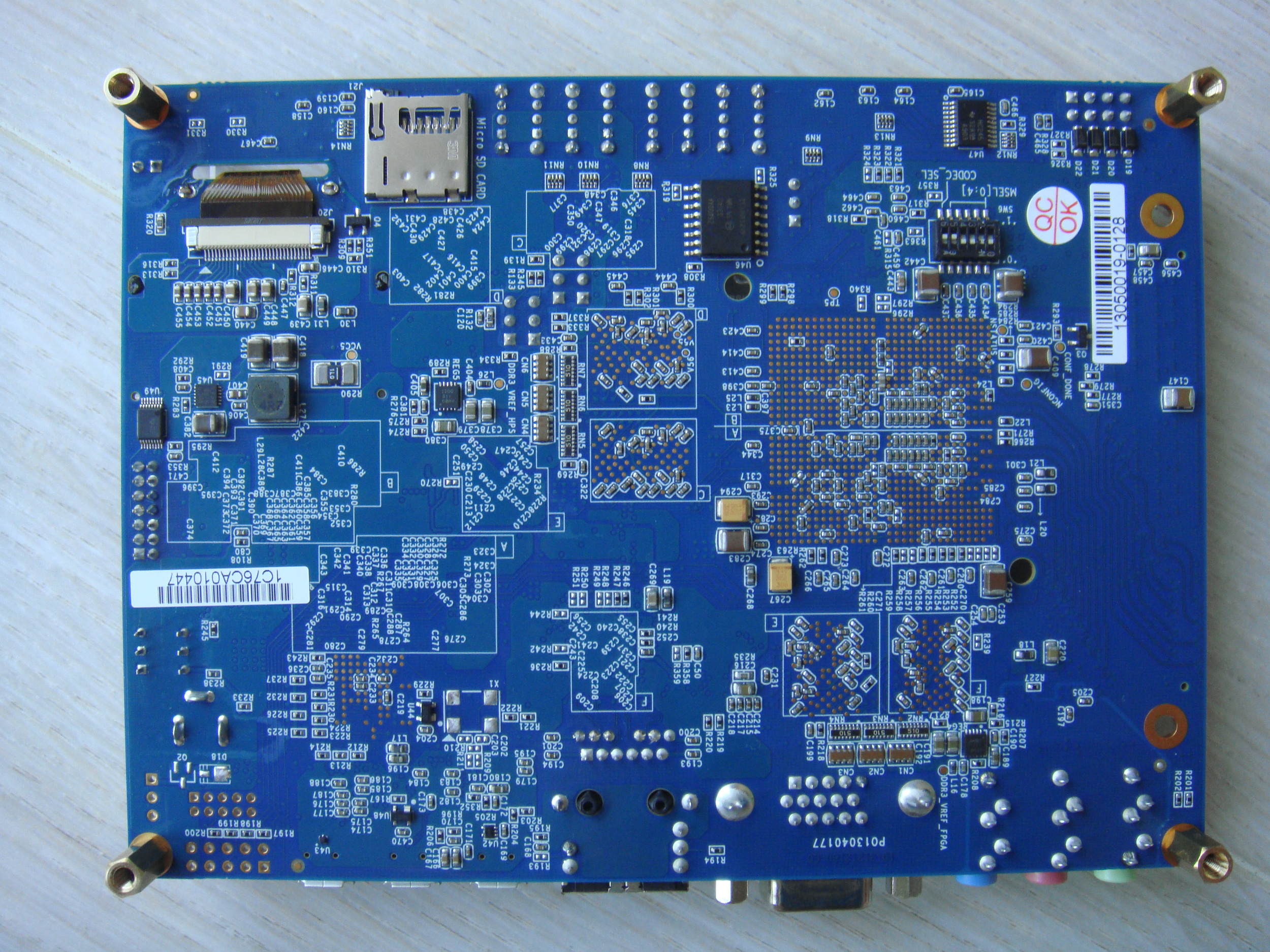
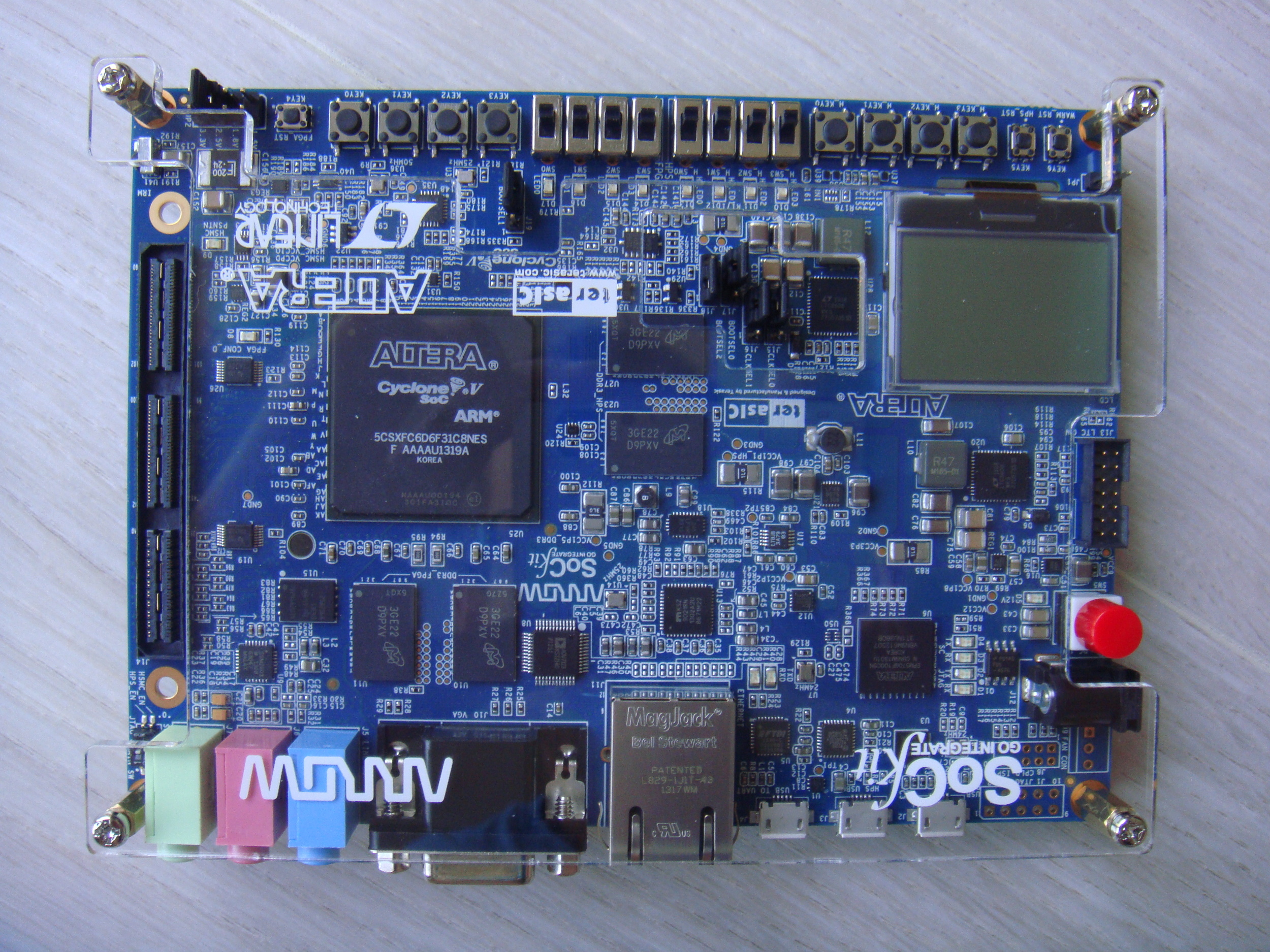
And below, the front and bottom of the SoC Kit evaluation board:


Very interesting article and a great board.
Thank you
I just didn’t have time to moderate it yet. We would get too much junk on the blog if we didn’t moderate messages.
Michael.
Hello sir,
Thank you the workshop , I was trying SW lab , I am getting as follows,
sdram.c:In function ‘sdram_mmr_init_full’:
sdram.c:1043:4:error:’$’ undeclared
sdram.c:1043:4:error:expected ‘)’ before ‘{‘ token
….
I feel like some environment variable need to be set please reply back soon, i am stuck here from 2 days,..
You should ask Altera to support you. We are not the creators of these labs!
I have the same problem. I solved it to use the bsp-editor generator with the files from the HW_lab Workshop instead the SW_lab. Perhaps the toolchains differ from the workshop (13.0.0) and the actual Altera Quartus II (13.0.1 SP1).
Philipp
Hello Phil,
I have the same problems and looking for solution. I want to use the files from HW_Lab too but I don’t know which files to include. Could you tell me what files are needed for the bsp or I just include xml file?
Thank you very much
Best,
Tony
Hi, I am an Altera FAE in the states…have you guys seen our portal for all things soc? It should have update materials for all the labs that go with this kit, including our own kit. Our site is http://www.rocketboards.org, and take a look under the resources and projects section.
BTW, where are you seeing that sdram failure? in the bitbake process?
Hey Guys,
Does anybody has some information about the LCD on the board? I need to enable it… but I cannot find any driver or any reference manual to develop it by myself.
Thanks,
Fabrizio
Hi
Thanks you so much for your workshop documentation
Is this possible to access the FPGA peripherals from the HPS? For example toggle the LED status which is not connected to the HPS side
Is any tutorial video available online related to the workshop and demonstrations?
There are some HPS-FPGA communication bridges (like AXI) but I am not sure if it is only for memory purposes. This may help:
http://www.altera.com/literature/hb/cyclone-v/cv_54005.pdf
They do not seem to have these workshops anymore (atleast in Canada). Thank you so much for sharing the workshop material.